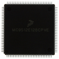
MC9S12E128CPVE Freescale Semiconductor, MC9S12E128CPVE Datasheet - Page 211

MC9S12E128CPVE
Manufacturer Part Number
MC9S12E128CPVE
Description
IC MCU 128K FLASH 25MHZ 112-LQFP
Manufacturer
Freescale Semiconductor
Series
HCS12r
Specifications of MC9S12E128CPVE
Core Processor
HCS12
Core Size
16-Bit
Speed
25MHz
Connectivity
EBI/EMI, I²C, SCI, SPI
Peripherals
POR, PWM, WDT
Number Of I /o
91
Program Memory Size
128KB (128K x 8)
Program Memory Type
FLASH
Ram Size
8K x 8
Voltage - Supply (vcc/vdd)
2.35 V ~ 2.75 V
Data Converters
A/D 16x10b; D/A 2x8b
Oscillator Type
Internal
Operating Temperature
-40°C ~ 85°C
Package / Case
112-LQFP
Processor Series
S12E
Core
HCS12
Data Bus Width
16 bit
Data Ram Size
8 KB
Interface Type
SCI/SPI
Maximum Clock Frequency
25 MHz
Number Of Programmable I/os
92
Number Of Timers
12
Operating Supply Voltage
3.135 V to 5.5 V
Maximum Operating Temperature
+ 85 C
Mounting Style
SMD/SMT
3rd Party Development Tools
EWHCS12
Minimum Operating Temperature
- 40 C
On-chip Adc
16-ch x 10-bit
On-chip Dac
2-ch x 8-bit
Controller Family/series
HCS12/S12X
No. Of I/o's
90
Ram Memory Size
8KB
Cpu Speed
25MHz
No. Of Timers
4
Embedded Interface Type
I2C, SCI, SPI
Rohs Compliant
Yes
For Use With
M68EVB912E128 - BOARD EVAL FOR MC9S12E128/64
Lead Free Status / RoHS Status
Lead free / RoHS Compliant
Eeprom Size
-
Lead Free Status / Rohs Status
Lead free / RoHS Compliant
Available stocks
Company
Part Number
Manufacturer
Quantity
Price
Company:
Part Number:
MC9S12E128CPVE
Manufacturer:
Freescale Semiconductor
Quantity:
10 000
- Current page: 211 of 606
- Download datasheet (4Mb)
Read: always read $00 in normal modes
Write: unimplemented in normal modes
6.3.2.3
This register controls power down, interrupt and external trigger. Writes to this register will abort current
conversion sequence but will not start a new sequence.
Read: Anytime
Write: Anytime
Freescale Semiconductor
ETRIGLE
Reset
ETRIGP
ETRIGE
ADPU
AFFC
AWAI
Field
W
7
6
5
4
3
2
R
ADPU
ATD Control Register 2 (ATDCTL2)
0
7
ATD Power Down — This bit provides on/off control over the ATD10B16C block allowing reduced MCU power
consumption. Because analog electronic is turned off when powered down, the ATD requires a recovery time
period after ADPU bit is enabled.
0 Power down ATD
1 Normal ATD functionality
ATD Fast Flag Clear All
0 ATD flag clearing operates normally (read the status register ATDSTAT1 before reading the result register
1 Changes all ATD conversion complete flags to a fast clear sequence. Any access to a result register will
ATD Power Down in Wait Mode — When entering Wait Mode this bit provides on/off control over the
ATD10B16C block allowing reduced MCU power. Because analog electronic is turned off when powered down,
the ATD requires a recovery time period after exit from Wait mode.
0 ATD continues to run in Wait mode
1 Halt conversion and power down ATD during Wait mode
External Trigger Level/Edge Control — This bit controls the sensitivity of the external trigger signal. See
Table 6-3
External Trigger Polarity — This bit controls the polarity of the external trigger signal. See
details.
External Trigger Mode Enable — This bit enables the external trigger on ATD channel 15. The external trigger
allows to synchronize the start of conversion with external events.
0 Disable external trigger
1 Enable external trigger
to clear the associate CCF flag).
cause the associate CCF flag to clear automatically.
After exiting Wait mode with an interrupt conversion will resume. But due to the recovery time the result of
this conversion should be ignored.
= Unimplemented or Reserved
for details.
AFFC
0
6
Figure 6-5. ATD Control Register 2 (ATDCTL2)
Table 6-2. ATDCTL2 Field Descriptions
AWAI
MC9S12E128 Data Sheet, Rev. 1.07
0
5
ETRIGLE
0
4
Description
ETRIGP
Chapter 6 Analog-to-Digital Converter (ATD10B16CV2)
0
3
ETRIGE
0
2
ASCIE
0
1
Table 6-3
ASCIF
for
0
0
211
Related parts for MC9S12E128CPVE
Image
Part Number
Description
Manufacturer
Datasheet
Request
R
Part Number:
Description:
Manufacturer:
Freescale Semiconductor, Inc
Datasheet:
Part Number:
Description:
Manufacturer:
Freescale Semiconductor, Inc
Datasheet:
Part Number:
Description:
Manufacturer:
Freescale Semiconductor, Inc
Datasheet:
Part Number:
Description:
Manufacturer:
Freescale Semiconductor, Inc
Datasheet:
Part Number:
Description:
Manufacturer:
Freescale Semiconductor, Inc
Datasheet:
Part Number:
Description:
Manufacturer:
Freescale Semiconductor, Inc
Datasheet:
Part Number:
Description:
Manufacturer:
Freescale Semiconductor, Inc
Datasheet:
Part Number:
Description:
Manufacturer:
Freescale Semiconductor, Inc
Datasheet:
Part Number:
Description:
Manufacturer:
Freescale Semiconductor, Inc
Datasheet:
Part Number:
Description:
Manufacturer:
Freescale Semiconductor, Inc
Datasheet:
Part Number:
Description:
Manufacturer:
Freescale Semiconductor, Inc
Datasheet:
Part Number:
Description:
Manufacturer:
Freescale Semiconductor, Inc
Datasheet:
Part Number:
Description:
Manufacturer:
Freescale Semiconductor, Inc
Datasheet:
Part Number:
Description:
Manufacturer:
Freescale Semiconductor, Inc
Datasheet:
Part Number:
Description:
Manufacturer:
Freescale Semiconductor, Inc
Datasheet:


