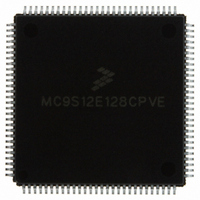
MC9S12E128CPVE Freescale Semiconductor, MC9S12E128CPVE Datasheet - Page 324

MC9S12E128CPVE
Manufacturer Part Number
MC9S12E128CPVE
Description
IC MCU 128K FLASH 25MHZ 112-LQFP
Manufacturer
Freescale Semiconductor
Series
HCS12r
Specifications of MC9S12E128CPVE
Core Processor
HCS12
Core Size
16-Bit
Speed
25MHz
Connectivity
EBI/EMI, I²C, SCI, SPI
Peripherals
POR, PWM, WDT
Number Of I /o
91
Program Memory Size
128KB (128K x 8)
Program Memory Type
FLASH
Ram Size
8K x 8
Voltage - Supply (vcc/vdd)
2.35 V ~ 2.75 V
Data Converters
A/D 16x10b; D/A 2x8b
Oscillator Type
Internal
Operating Temperature
-40°C ~ 85°C
Package / Case
112-LQFP
Processor Series
S12E
Core
HCS12
Data Bus Width
16 bit
Data Ram Size
8 KB
Interface Type
SCI/SPI
Maximum Clock Frequency
25 MHz
Number Of Programmable I/os
92
Number Of Timers
12
Operating Supply Voltage
3.135 V to 5.5 V
Maximum Operating Temperature
+ 85 C
Mounting Style
SMD/SMT
3rd Party Development Tools
EWHCS12
Minimum Operating Temperature
- 40 C
On-chip Adc
16-ch x 10-bit
On-chip Dac
2-ch x 8-bit
Controller Family/series
HCS12/S12X
No. Of I/o's
90
Ram Memory Size
8KB
Cpu Speed
25MHz
No. Of Timers
4
Embedded Interface Type
I2C, SCI, SPI
Rohs Compliant
Yes
For Use With
M68EVB912E128 - BOARD EVAL FOR MC9S12E128/64
Lead Free Status / RoHS Status
Lead free / RoHS Compliant
Eeprom Size
-
Lead Free Status / Rohs Status
Lead free / RoHS Compliant
Available stocks
Company
Part Number
Manufacturer
Quantity
Price
Company:
Part Number:
MC9S12E128CPVE
Manufacturer:
Freescale Semiconductor
Quantity:
10 000
- Current page: 324 of 606
- Download datasheet (4Mb)
Chapter 11 Pulse Width Modulator with Fault Protection (PMF15B6CV2)
11.1.2
Care must be exercised when using this module in the modes listed in
in their inactive states in stop mode, and optionally under WAIT and freeze modes. PWM outputs will be
reactivated (assuming they were active to begin with) when these modes are exited.
11.1.3
Figure 11-1
The Mux/Swap/Current Sense block is tightly integrated with the dead time insertion block . This detail
is shown in
324
Figure
Modes of Operation
Block Diagrams
provides an overview of the PMF module.
It is possible to have both channels of a complementary pair to be high. For
example, if the TOPNEGA (negative polarity for PWM0), BOTNEGA
(negative polarity for PWM1), MASK0, and MASK1 bits are set, both the
PWM complementary outputs of generator A will be high. See
Section 11.3.2.2, “PMF Configure 1 Register (PMFCFG1)”
description of TOPNEG and BOTNEG bits, and
Configure 2 Register (PMFCFG2)”
MSK1 bits.
Freeze
Mode
Stop
Wait
11-2.
Table 11-1. Modes When PWM Operation is Restricted
MC9S12E128 Data Sheet, Rev. 1.07
PWM outputs are disabled as a function of the PMFFRZ bit.
PWM outputs are disabled as a function of the PMFWAI bit.
NOTE
for the description of the MSK0 and
PWM outputs are disabled
Description
Section 11.3.2.3, “PMF
Table
11-1. PWM outputs are placed
for the
Freescale Semiconductor
Related parts for MC9S12E128CPVE
Image
Part Number
Description
Manufacturer
Datasheet
Request
R
Part Number:
Description:
Manufacturer:
Freescale Semiconductor, Inc
Datasheet:
Part Number:
Description:
Manufacturer:
Freescale Semiconductor, Inc
Datasheet:
Part Number:
Description:
Manufacturer:
Freescale Semiconductor, Inc
Datasheet:
Part Number:
Description:
Manufacturer:
Freescale Semiconductor, Inc
Datasheet:
Part Number:
Description:
Manufacturer:
Freescale Semiconductor, Inc
Datasheet:
Part Number:
Description:
Manufacturer:
Freescale Semiconductor, Inc
Datasheet:
Part Number:
Description:
Manufacturer:
Freescale Semiconductor, Inc
Datasheet:
Part Number:
Description:
Manufacturer:
Freescale Semiconductor, Inc
Datasheet:
Part Number:
Description:
Manufacturer:
Freescale Semiconductor, Inc
Datasheet:
Part Number:
Description:
Manufacturer:
Freescale Semiconductor, Inc
Datasheet:
Part Number:
Description:
Manufacturer:
Freescale Semiconductor, Inc
Datasheet:
Part Number:
Description:
Manufacturer:
Freescale Semiconductor, Inc
Datasheet:
Part Number:
Description:
Manufacturer:
Freescale Semiconductor, Inc
Datasheet:
Part Number:
Description:
Manufacturer:
Freescale Semiconductor, Inc
Datasheet:
Part Number:
Description:
Manufacturer:
Freescale Semiconductor, Inc
Datasheet:


