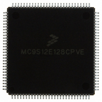
MC9S12E128CPVE Freescale Semiconductor, MC9S12E128CPVE Datasheet - Page 400

MC9S12E128CPVE
Manufacturer Part Number
MC9S12E128CPVE
Description
IC MCU 128K FLASH 25MHZ 112-LQFP
Manufacturer
Freescale Semiconductor
Series
HCS12r
Specifications of MC9S12E128CPVE
Core Processor
HCS12
Core Size
16-Bit
Speed
25MHz
Connectivity
EBI/EMI, I²C, SCI, SPI
Peripherals
POR, PWM, WDT
Number Of I /o
91
Program Memory Size
128KB (128K x 8)
Program Memory Type
FLASH
Ram Size
8K x 8
Voltage - Supply (vcc/vdd)
2.35 V ~ 2.75 V
Data Converters
A/D 16x10b; D/A 2x8b
Oscillator Type
Internal
Operating Temperature
-40°C ~ 85°C
Package / Case
112-LQFP
Processor Series
S12E
Core
HCS12
Data Bus Width
16 bit
Data Ram Size
8 KB
Interface Type
SCI/SPI
Maximum Clock Frequency
25 MHz
Number Of Programmable I/os
92
Number Of Timers
12
Operating Supply Voltage
3.135 V to 5.5 V
Maximum Operating Temperature
+ 85 C
Mounting Style
SMD/SMT
3rd Party Development Tools
EWHCS12
Minimum Operating Temperature
- 40 C
On-chip Adc
16-ch x 10-bit
On-chip Dac
2-ch x 8-bit
Controller Family/series
HCS12/S12X
No. Of I/o's
90
Ram Memory Size
8KB
Cpu Speed
25MHz
No. Of Timers
4
Embedded Interface Type
I2C, SCI, SPI
Rohs Compliant
Yes
For Use With
M68EVB912E128 - BOARD EVAL FOR MC9S12E128/64
Lead Free Status / RoHS Status
Lead free / RoHS Compliant
Eeprom Size
-
Lead Free Status / Rohs Status
Lead free / RoHS Compliant
Available stocks
Company
Part Number
Manufacturer
Quantity
Price
Company:
Part Number:
MC9S12E128CPVE
Manufacturer:
Freescale Semiconductor
Quantity:
10 000
- Current page: 400 of 606
- Download datasheet (4Mb)
Chapter 12 Pulse-Width Modulator (PWM8B6CV1)
Read: anytime
Write: anytime
12.3.2.14 PWM Channel Duty Registers (PWMDTYx)
There is a dedicated duty register for each channel. The value in this register determines the duty of the
associated PWM channel. The duty value is compared to the counter and if it is equal to the counter value
a match occurs and the output changes state.
The duty registers for each channel are double buffered so that if they change while the channel is enabled,
the change will NOT take effect until one of the following occurs:
In this way, the output of the PWM will always be either the old duty waveform or the new duty waveform,
not some variation in between. If the channel is not enabled, then writes to the duty register will go directly
to the latches as well as the buffer.
Reference
To calculate the output duty cycle (high time as a % of period) for a particular channel:
400
Reset
•
•
•
•
•
•
W
R
The effective period ends
The counter is written (counter resets to 0x0000)
The channel is disabled
Polarity = 0 (PPOLx = 0)
Polarity = 1 (PPOLx = 1)
For boundary case programming values, please refer to
Duty cycle = [(PWMPERx PWMDTYx)/PWMPERx] * 100%
Duty cycle = [PWMDTYx / PWMPERx] * 100%
Section 12.4.2.3, “PWM Period and Duty,”
Bit 7
0
7
Reads of this register return the most recent value written. Reads do not
necessarily return the value of the currently active duty due to the double
buffering scheme.
Depending on the polarity bit, the duty registers will contain the count of
either the high time or the low time. If the polarity bit is 1, the output starts
high and then goes low when the duty count is reached, so the duty registers
contain a count of the high time. If the polarity bit is 0, the output starts low
and then goes high when the duty count is reached, so the duty registers
contain a count of the low time.
Figure 12-26. PWM Channel Period Registers (PWMPER5)
6
0
6
MC9S12E128 Data Sheet, Rev. 1.07
5
0
5
NOTE
NOTE
4
0
4
for more information.
3
0
Section 12.4.2.8, “PWM Boundary Cases.”
3
2
0
2
Freescale Semiconductor
1
0
1
Bit 0
0
0
Related parts for MC9S12E128CPVE
Image
Part Number
Description
Manufacturer
Datasheet
Request
R
Part Number:
Description:
Manufacturer:
Freescale Semiconductor, Inc
Datasheet:
Part Number:
Description:
Manufacturer:
Freescale Semiconductor, Inc
Datasheet:
Part Number:
Description:
Manufacturer:
Freescale Semiconductor, Inc
Datasheet:
Part Number:
Description:
Manufacturer:
Freescale Semiconductor, Inc
Datasheet:
Part Number:
Description:
Manufacturer:
Freescale Semiconductor, Inc
Datasheet:
Part Number:
Description:
Manufacturer:
Freescale Semiconductor, Inc
Datasheet:
Part Number:
Description:
Manufacturer:
Freescale Semiconductor, Inc
Datasheet:
Part Number:
Description:
Manufacturer:
Freescale Semiconductor, Inc
Datasheet:
Part Number:
Description:
Manufacturer:
Freescale Semiconductor, Inc
Datasheet:
Part Number:
Description:
Manufacturer:
Freescale Semiconductor, Inc
Datasheet:
Part Number:
Description:
Manufacturer:
Freescale Semiconductor, Inc
Datasheet:
Part Number:
Description:
Manufacturer:
Freescale Semiconductor, Inc
Datasheet:
Part Number:
Description:
Manufacturer:
Freescale Semiconductor, Inc
Datasheet:
Part Number:
Description:
Manufacturer:
Freescale Semiconductor, Inc
Datasheet:
Part Number:
Description:
Manufacturer:
Freescale Semiconductor, Inc
Datasheet:


