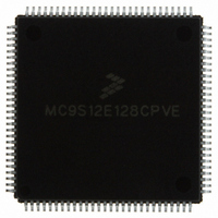
MC9S12E128CPVE Freescale Semiconductor, MC9S12E128CPVE Datasheet - Page 458

MC9S12E128CPVE
Manufacturer Part Number
MC9S12E128CPVE
Description
IC MCU 128K FLASH 25MHZ 112-LQFP
Manufacturer
Freescale Semiconductor
Series
HCS12r
Specifications of MC9S12E128CPVE
Core Processor
HCS12
Core Size
16-Bit
Speed
25MHz
Connectivity
EBI/EMI, I²C, SCI, SPI
Peripherals
POR, PWM, WDT
Number Of I /o
91
Program Memory Size
128KB (128K x 8)
Program Memory Type
FLASH
Ram Size
8K x 8
Voltage - Supply (vcc/vdd)
2.35 V ~ 2.75 V
Data Converters
A/D 16x10b; D/A 2x8b
Oscillator Type
Internal
Operating Temperature
-40°C ~ 85°C
Package / Case
112-LQFP
Processor Series
S12E
Core
HCS12
Data Bus Width
16 bit
Data Ram Size
8 KB
Interface Type
SCI/SPI
Maximum Clock Frequency
25 MHz
Number Of Programmable I/os
92
Number Of Timers
12
Operating Supply Voltage
3.135 V to 5.5 V
Maximum Operating Temperature
+ 85 C
Mounting Style
SMD/SMT
3rd Party Development Tools
EWHCS12
Minimum Operating Temperature
- 40 C
On-chip Adc
16-ch x 10-bit
On-chip Dac
2-ch x 8-bit
Controller Family/series
HCS12/S12X
No. Of I/o's
90
Ram Memory Size
8KB
Cpu Speed
25MHz
No. Of Timers
4
Embedded Interface Type
I2C, SCI, SPI
Rohs Compliant
Yes
For Use With
M68EVB912E128 - BOARD EVAL FOR MC9S12E128/64
Lead Free Status / RoHS Status
Lead free / RoHS Compliant
Eeprom Size
-
Lead Free Status / Rohs Status
Lead free / RoHS Compliant
Available stocks
Company
Part Number
Manufacturer
Quantity
Price
Company:
Part Number:
MC9S12E128CPVE
Manufacturer:
Freescale Semiconductor
Quantity:
10 000
- Current page: 458 of 606
- Download datasheet (4Mb)
Chapter 15 Background Debug Module (BDMV4)
The BDM hardware commands are listed in
NOTE:
The READ_BD and WRITE_BD commands allow access to the BDM register locations. These locations
are not normally in the system memory map but share addresses with the application in memory. To
distinguish between physical memory locations that share the same address, BDM memory resources are
enabled just for the READ_BD and WRITE_BD access cycle. This allows the BDM to access BDM
locations unobtrusively, even if the addresses conflict with the application memory map.
15.4.4
Firmware commands are used to access and manipulate CPU resources. The system must be in active
BDM to execute standard BDM firmware commands, see
BDM.” Normal instruction execution is suspended while the CPU executes the firmware located in the
standard BDM firmware lookup table. The hardware command BACKGROUND is the usual way to
activate BDM.
As the system enters active BDM, the standard BDM firmware lookup table and BDM registers become
visible in the on-chip memory map at 0xFF00–0xFFFF, and the CPU begins executing the standard BDM
458
BACKGROUND
ACK_ENABLE
ACK_DISABLE
READ_BD_BYTE
READ_BD_WORD
READ_BYTE
READ_WORD
WRITE_BD_BYTE
WRITE_BD_WORD
WRITE_BYTE
WRITE_WORD
If enabled, ACK will occur when data is ready for transmission for all BDM READ commands and will occur after the write is
complete for all BDM WRITE commands.
Command
Standard BDM Firmware Commands
Opcode
(hex)
CC
EC
D5
D6
E4
E0
E8
C4
C0
C8
90
16-bit address
16-bit data out
16-bit address
16-bit data out
16-bit address
16-bit data out
16-bit address
16-bit data out
16-bit address
16-bit address
16-bit address
16-bit address
16-bit data in
16-bit data in
16-bit data in
16-bit data in
None
None
None
Data
Table 15-5. Hardware Commands
MC9S12E128 Data Sheet, Rev. 1.07
Table
Enter background mode if firmware is enabled. If enabled, an ACK will
be issued when the part enters active background mode.
Enable handshake. Issues an ACK pulse after the command is
executed.
Disable handshake. This command does not issue an ACK pulse.
Read from memory with standard BDM firmware lookup table in map.
Odd address data on low byte; even address data on high byte.
Read from memory with standard BDM firmware lookup table in map.
Must be aligned access.
Read from memory with standard BDM firmware lookup table out of
map. Odd address data on low byte; even address data on high byte.
Read from memory with standard BDM firmware lookup table out of
map. Must be aligned access.
Write to memory with standard BDM firmware lookup table in map. Odd
address data on low byte; even address data on high byte.
Write to memory with standard BDM firmware lookup table in map. Must
be aligned access.
Write to memory with standard BDM firmware lookup table out of map.
Odd address data on low byte; even address data on high byte.
Write to memory with standard BDM firmware lookup table out of map.
Must be aligned access.
15-5.
Section 15.4.2, “Enabling and Activating
Description
Freescale Semiconductor
Related parts for MC9S12E128CPVE
Image
Part Number
Description
Manufacturer
Datasheet
Request
R
Part Number:
Description:
Manufacturer:
Freescale Semiconductor, Inc
Datasheet:
Part Number:
Description:
Manufacturer:
Freescale Semiconductor, Inc
Datasheet:
Part Number:
Description:
Manufacturer:
Freescale Semiconductor, Inc
Datasheet:
Part Number:
Description:
Manufacturer:
Freescale Semiconductor, Inc
Datasheet:
Part Number:
Description:
Manufacturer:
Freescale Semiconductor, Inc
Datasheet:
Part Number:
Description:
Manufacturer:
Freescale Semiconductor, Inc
Datasheet:
Part Number:
Description:
Manufacturer:
Freescale Semiconductor, Inc
Datasheet:
Part Number:
Description:
Manufacturer:
Freescale Semiconductor, Inc
Datasheet:
Part Number:
Description:
Manufacturer:
Freescale Semiconductor, Inc
Datasheet:
Part Number:
Description:
Manufacturer:
Freescale Semiconductor, Inc
Datasheet:
Part Number:
Description:
Manufacturer:
Freescale Semiconductor, Inc
Datasheet:
Part Number:
Description:
Manufacturer:
Freescale Semiconductor, Inc
Datasheet:
Part Number:
Description:
Manufacturer:
Freescale Semiconductor, Inc
Datasheet:
Part Number:
Description:
Manufacturer:
Freescale Semiconductor, Inc
Datasheet:
Part Number:
Description:
Manufacturer:
Freescale Semiconductor, Inc
Datasheet:


