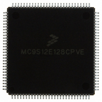
MC9S12E128CPVE Freescale Semiconductor, MC9S12E128CPVE Datasheet - Page 477

MC9S12E128CPVE
Manufacturer Part Number
MC9S12E128CPVE
Description
IC MCU 128K FLASH 25MHZ 112-LQFP
Manufacturer
Freescale Semiconductor
Series
HCS12r
Specifications of MC9S12E128CPVE
Core Processor
HCS12
Core Size
16-Bit
Speed
25MHz
Connectivity
EBI/EMI, I²C, SCI, SPI
Peripherals
POR, PWM, WDT
Number Of I /o
91
Program Memory Size
128KB (128K x 8)
Program Memory Type
FLASH
Ram Size
8K x 8
Voltage - Supply (vcc/vdd)
2.35 V ~ 2.75 V
Data Converters
A/D 16x10b; D/A 2x8b
Oscillator Type
Internal
Operating Temperature
-40°C ~ 85°C
Package / Case
112-LQFP
Processor Series
S12E
Core
HCS12
Data Bus Width
16 bit
Data Ram Size
8 KB
Interface Type
SCI/SPI
Maximum Clock Frequency
25 MHz
Number Of Programmable I/os
92
Number Of Timers
12
Operating Supply Voltage
3.135 V to 5.5 V
Maximum Operating Temperature
+ 85 C
Mounting Style
SMD/SMT
3rd Party Development Tools
EWHCS12
Minimum Operating Temperature
- 40 C
On-chip Adc
16-ch x 10-bit
On-chip Dac
2-ch x 8-bit
Controller Family/series
HCS12/S12X
No. Of I/o's
90
Ram Memory Size
8KB
Cpu Speed
25MHz
No. Of Timers
4
Embedded Interface Type
I2C, SCI, SPI
Rohs Compliant
Yes
For Use With
M68EVB912E128 - BOARD EVAL FOR MC9S12E128/64
Lead Free Status / RoHS Status
Lead free / RoHS Compliant
Eeprom Size
-
Lead Free Status / Rohs Status
Lead free / RoHS Compliant
Available stocks
Company
Part Number
Manufacturer
Quantity
Price
Company:
Part Number:
MC9S12E128CPVE
Manufacturer:
Freescale Semiconductor
Quantity:
10 000
- Current page: 477 of 606
- Download datasheet (4Mb)
16.2
The DBG sub-module relies on the external bus interface (generally the MEBI) when the DBG is matching
on the external bus.
The tag pins in
Freescale Semiconductor
PE3/LSTRB/ TAGLO
BKGD/MODC/
CPU PROGRAM COUNTER
INSTRUCTION
Pin Name
LAST CYCLE
BUS CLOCK
TAGHI
External Signal Description
WRITE DATA BUS
READ DATA BUS
ADDRESS BUS
WRITE DATA BUS
READ DATA BUS
READ/WRITE
DBG MODE ENABLE
CHANGE-OF-FLOW
INDICATORS
MCU IN BDM
DBG READ DATA BUS
Table 16-1
READ/WRITE
REGISTER
Table 16-1. External System Pins Associated with DBG and MEBI
Pin Functions
TAGLO
TAGHI
(part of the MEBI) may also be a part of the breakpoint operation.
Figure 16-2. DBG Block Diagram in DBG Mode
M
U
X
When instruction tagging is on, a 0 at the falling edge of E tags the high half of the
instruction word being read into the instruction queue.
In expanded wide mode or emulation narrow modes, when instruction tagging is on
and low strobe is enabled, a 0 at the falling edge of E tags the low half of the
instruction word being read into the instruction queue.
MC9S12E128 Data Sheet, Rev. 1.07
M
U
X
INSTRUCTION
ADDRESS/DATA/CONTROL
ADDRESS
M
U
X
COMPARATOR A
COMPARATOR B
COMPARATOR C
LAST
REGISTERS
64 x 16 BIT
REGISTER
CAPTURE
PROFILE
BUFFER
TRACE
WORD
Description
CONTROL
MATCH_A
MATCH_B
MATCH_C
LOOP1
EVENT ONLY
POINTER
M
U
X
STORE
DETAIL
PROFILE CAPTURE MODE
Chapter 16 Debug Module (DBGV1)
CONTROL
TRACER
OR PROFILING DATA
BUFFER
LOGIC
TRACE BUFFER
TAG
FORCE
477
Related parts for MC9S12E128CPVE
Image
Part Number
Description
Manufacturer
Datasheet
Request
R
Part Number:
Description:
Manufacturer:
Freescale Semiconductor, Inc
Datasheet:
Part Number:
Description:
Manufacturer:
Freescale Semiconductor, Inc
Datasheet:
Part Number:
Description:
Manufacturer:
Freescale Semiconductor, Inc
Datasheet:
Part Number:
Description:
Manufacturer:
Freescale Semiconductor, Inc
Datasheet:
Part Number:
Description:
Manufacturer:
Freescale Semiconductor, Inc
Datasheet:
Part Number:
Description:
Manufacturer:
Freescale Semiconductor, Inc
Datasheet:
Part Number:
Description:
Manufacturer:
Freescale Semiconductor, Inc
Datasheet:
Part Number:
Description:
Manufacturer:
Freescale Semiconductor, Inc
Datasheet:
Part Number:
Description:
Manufacturer:
Freescale Semiconductor, Inc
Datasheet:
Part Number:
Description:
Manufacturer:
Freescale Semiconductor, Inc
Datasheet:
Part Number:
Description:
Manufacturer:
Freescale Semiconductor, Inc
Datasheet:
Part Number:
Description:
Manufacturer:
Freescale Semiconductor, Inc
Datasheet:
Part Number:
Description:
Manufacturer:
Freescale Semiconductor, Inc
Datasheet:
Part Number:
Description:
Manufacturer:
Freescale Semiconductor, Inc
Datasheet:
Part Number:
Description:
Manufacturer:
Freescale Semiconductor, Inc
Datasheet:


