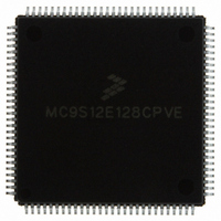
MC9S12E128CPVE Freescale Semiconductor, MC9S12E128CPVE Datasheet - Page 496

MC9S12E128CPVE
Manufacturer Part Number
MC9S12E128CPVE
Description
IC MCU 128K FLASH 25MHZ 112-LQFP
Manufacturer
Freescale Semiconductor
Series
HCS12r
Specifications of MC9S12E128CPVE
Core Processor
HCS12
Core Size
16-Bit
Speed
25MHz
Connectivity
EBI/EMI, I²C, SCI, SPI
Peripherals
POR, PWM, WDT
Number Of I /o
91
Program Memory Size
128KB (128K x 8)
Program Memory Type
FLASH
Ram Size
8K x 8
Voltage - Supply (vcc/vdd)
2.35 V ~ 2.75 V
Data Converters
A/D 16x10b; D/A 2x8b
Oscillator Type
Internal
Operating Temperature
-40°C ~ 85°C
Package / Case
112-LQFP
Processor Series
S12E
Core
HCS12
Data Bus Width
16 bit
Data Ram Size
8 KB
Interface Type
SCI/SPI
Maximum Clock Frequency
25 MHz
Number Of Programmable I/os
92
Number Of Timers
12
Operating Supply Voltage
3.135 V to 5.5 V
Maximum Operating Temperature
+ 85 C
Mounting Style
SMD/SMT
3rd Party Development Tools
EWHCS12
Minimum Operating Temperature
- 40 C
On-chip Adc
16-ch x 10-bit
On-chip Dac
2-ch x 8-bit
Controller Family/series
HCS12/S12X
No. Of I/o's
90
Ram Memory Size
8KB
Cpu Speed
25MHz
No. Of Timers
4
Embedded Interface Type
I2C, SCI, SPI
Rohs Compliant
Yes
For Use With
M68EVB912E128 - BOARD EVAL FOR MC9S12E128/64
Lead Free Status / RoHS Status
Lead free / RoHS Compliant
Eeprom Size
-
Lead Free Status / Rohs Status
Lead free / RoHS Compliant
Available stocks
Company
Part Number
Manufacturer
Quantity
Price
Company:
Part Number:
MC9S12E128CPVE
Manufacturer:
Freescale Semiconductor
Quantity:
10 000
- Current page: 496 of 606
- Download datasheet (4Mb)
Chapter 16 Debug Module (DBGV1)
control (TBC) block. When PAGSEL = 01, registers DBGCAX, DBGCBX, and DBGCCX are used to
match the upper addresses as shown in
16.4.2.1.1
Read or write comparisons are useful only with TRGSEL = 0, because only opcodes should be tagged as
they are “read” from memory. RWAEN and RWBEN are ignored when TRGSEL = 1.
In full modes (“A and B” and “A and not B”) RWAEN and RWA are used to select read or write
comparisons for both comparators A and B.
the DBGCB comparison conditions. The RWBEN and RWB bits are not used and are ignored in full
modes.
16.4.2.1.2
The TRGSEL bit in DBGC1 is used to determine the triggering condition in DBG mode. TRGSEL applies
to both trigger A and B except in the event only trigger modes. By setting TRGSEL, the comparators A
and B will qualify a match with the output of opcode tracking logic and a trigger occurs before the tagged
instruction executes (tagged-type trigger). With the TRGSEL bit cleared, a comparator match forces a
trigger when the matching condition occurs (force-type trigger).
16.4.2.2
The TBC is the main controller for the DBG module. Its function is to decide whether data should be stored
in the trace buffer based on the trigger mode and the match signals from the comparator. The TBC also
determines whether a request to break the CPU should occur.
496
Trace Buffer Control (TBC)
RWAEN bit
If a tagged-type C breakpoint is set at the same address as an A/B
tagged-type trigger (including the initial entry in an inside or outside range
trigger), the C breakpoint will have priority and the trigger will not be
recognized.
Read or Write Comparison
Trigger Selection
If the TRGSEL is set, the address stored in the comparator match address
registers must be an opcode address for the trigger to occur.
0
0
1
1
1
1
Table 16-24. Read or Write Comparison Logic Table
RWA bit
x
x
0
0
1
1
MC9S12E128 Data Sheet, Rev. 1.07
Table
Table 16-24
RW signal
16-11.
0
1
0
1
0
1
NOTE
NOTE
shows the effect for RWAEN, RWA, and RW on
No data bus compare since RW=1
No data bus compare since RW=0
Write data bus
Read data bus
Write data bus
Read data bus
Comment
Freescale Semiconductor
Related parts for MC9S12E128CPVE
Image
Part Number
Description
Manufacturer
Datasheet
Request
R
Part Number:
Description:
Manufacturer:
Freescale Semiconductor, Inc
Datasheet:
Part Number:
Description:
Manufacturer:
Freescale Semiconductor, Inc
Datasheet:
Part Number:
Description:
Manufacturer:
Freescale Semiconductor, Inc
Datasheet:
Part Number:
Description:
Manufacturer:
Freescale Semiconductor, Inc
Datasheet:
Part Number:
Description:
Manufacturer:
Freescale Semiconductor, Inc
Datasheet:
Part Number:
Description:
Manufacturer:
Freescale Semiconductor, Inc
Datasheet:
Part Number:
Description:
Manufacturer:
Freescale Semiconductor, Inc
Datasheet:
Part Number:
Description:
Manufacturer:
Freescale Semiconductor, Inc
Datasheet:
Part Number:
Description:
Manufacturer:
Freescale Semiconductor, Inc
Datasheet:
Part Number:
Description:
Manufacturer:
Freescale Semiconductor, Inc
Datasheet:
Part Number:
Description:
Manufacturer:
Freescale Semiconductor, Inc
Datasheet:
Part Number:
Description:
Manufacturer:
Freescale Semiconductor, Inc
Datasheet:
Part Number:
Description:
Manufacturer:
Freescale Semiconductor, Inc
Datasheet:
Part Number:
Description:
Manufacturer:
Freescale Semiconductor, Inc
Datasheet:
Part Number:
Description:
Manufacturer:
Freescale Semiconductor, Inc
Datasheet:


