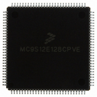
MC9S12E128CPVE Freescale Semiconductor, MC9S12E128CPVE Datasheet - Page 540

MC9S12E128CPVE
Manufacturer Part Number
MC9S12E128CPVE
Description
IC MCU 128K FLASH 25MHZ 112-LQFP
Manufacturer
Freescale Semiconductor
Series
HCS12r
Specifications of MC9S12E128CPVE
Core Processor
HCS12
Core Size
16-Bit
Speed
25MHz
Connectivity
EBI/EMI, I²C, SCI, SPI
Peripherals
POR, PWM, WDT
Number Of I /o
91
Program Memory Size
128KB (128K x 8)
Program Memory Type
FLASH
Ram Size
8K x 8
Voltage - Supply (vcc/vdd)
2.35 V ~ 2.75 V
Data Converters
A/D 16x10b; D/A 2x8b
Oscillator Type
Internal
Operating Temperature
-40°C ~ 85°C
Package / Case
112-LQFP
Processor Series
S12E
Core
HCS12
Data Bus Width
16 bit
Data Ram Size
8 KB
Interface Type
SCI/SPI
Maximum Clock Frequency
25 MHz
Number Of Programmable I/os
92
Number Of Timers
12
Operating Supply Voltage
3.135 V to 5.5 V
Maximum Operating Temperature
+ 85 C
Mounting Style
SMD/SMT
3rd Party Development Tools
EWHCS12
Minimum Operating Temperature
- 40 C
On-chip Adc
16-ch x 10-bit
On-chip Dac
2-ch x 8-bit
Controller Family/series
HCS12/S12X
No. Of I/o's
90
Ram Memory Size
8KB
Cpu Speed
25MHz
No. Of Timers
4
Embedded Interface Type
I2C, SCI, SPI
Rohs Compliant
Yes
For Use With
M68EVB912E128 - BOARD EVAL FOR MC9S12E128/64
Lead Free Status / RoHS Status
Lead free / RoHS Compliant
Eeprom Size
-
Lead Free Status / Rohs Status
Lead free / RoHS Compliant
Available stocks
Company
Part Number
Manufacturer
Quantity
Price
Company:
Part Number:
MC9S12E128CPVE
Manufacturer:
Freescale Semiconductor
Quantity:
10 000
- Current page: 540 of 606
- Download datasheet (4Mb)
Chapter 18 Multiplexed External Bus Interface (MEBIV3)
18.4.3.1.5
Expanded narrow modes are intended to allow connection of single 8-bit external memory devices for
lower cost systems that do not need the performance of a full 16-bit external data bus. Accesses to internal
resources that have been mapped external (i.e. PORTA, PORTB, DDRA, DDRB, PORTE, DDRE, PEAR,
PUCR, RDRIV) will be accessed with a 16-bit data bus on Ports A and B. Accesses of 16-bit external
words to addresses which are normally mapped external will be broken into two separate 8-bit accesses
using Port A as an 8-bit data bus. Internal operations continue to use full 16-bit data paths. They are only
visible externally as 16-bit information if IVIS=1.
Ports A and B are configured as multiplexed address and data output ports. During external accesses,
address A15, data D15 and D7 are associated with PA7, address A0 is associated with PB0 and data D8
and D0 are associated with PA0. During internal visible accesses and accesses to internal resources that
have been mapped external, address A15 and data D15 is associated with PA7 and address A0 and data
D0 is associated with PB0.
The bus control related pins in Port E (PE7/NOACC, PE6/MODB/IPIPE1, PE5/MODA/IPIPE0,
PE4/ECLK, PE3/LSTRB/TAGLO, and PE2/R/W) are all configured to serve their bus control output
functions rather than general purpose I/O. Notice that writes to the bus control enable bits in the PEAR
register in emulation mode are restricted.
The main difference between special modes and normal modes is that some of the bus control and system
control signals cannot be written in emulation modes.
18.4.3.2
There are two special operating modes that correspond to normal operating modes. These operating modes
are commonly used in factory testing and system development.
18.4.3.2.1
When the MCU is reset in this mode, the background debug mode is enabled and active. The MCU does
not fetch the reset vector and execute application code as it would in other modes. Instead the active
background mode is in control of CPU execution and BDM firmware is waiting for additional serial
commands through the BKGD pin. When a serial command instructs the MCU to return to normal
execution, the system will be configured as described below unless the reset states of internal control
registers have been changed through background commands after the MCU was reset.
There is no external expansion bus after reset in this mode. Ports A and B are initially simple bidirectional
I/O pins that are configured as high-impedance inputs with internal pull resistors disabled; however,
writing to the mode select bits in the MODE register (which is allowed in special modes) can change this
after reset. All of the Port E pins (except PE4/ECLK) are initially configured as general purpose
high-impedance inputs with internal pull resistors enabled. PE4/ECLK is configured as the E clock output
in this mode.
The pins associated with Port E bits 6, 5, 3, and 2 cannot be configured for their alternate functions IPIPE1,
IPIPE0, LSTRB, and R/W while the MCU is in single chip modes. In single chip modes, the associated
540
Special Operating Modes
Emulation Expanded Narrow Mode
Special Single-Chip Mode
MC9S12E128 Data Sheet, Rev. 1.07
Freescale Semiconductor
Related parts for MC9S12E128CPVE
Image
Part Number
Description
Manufacturer
Datasheet
Request
R
Part Number:
Description:
Manufacturer:
Freescale Semiconductor, Inc
Datasheet:
Part Number:
Description:
Manufacturer:
Freescale Semiconductor, Inc
Datasheet:
Part Number:
Description:
Manufacturer:
Freescale Semiconductor, Inc
Datasheet:
Part Number:
Description:
Manufacturer:
Freescale Semiconductor, Inc
Datasheet:
Part Number:
Description:
Manufacturer:
Freescale Semiconductor, Inc
Datasheet:
Part Number:
Description:
Manufacturer:
Freescale Semiconductor, Inc
Datasheet:
Part Number:
Description:
Manufacturer:
Freescale Semiconductor, Inc
Datasheet:
Part Number:
Description:
Manufacturer:
Freescale Semiconductor, Inc
Datasheet:
Part Number:
Description:
Manufacturer:
Freescale Semiconductor, Inc
Datasheet:
Part Number:
Description:
Manufacturer:
Freescale Semiconductor, Inc
Datasheet:
Part Number:
Description:
Manufacturer:
Freescale Semiconductor, Inc
Datasheet:
Part Number:
Description:
Manufacturer:
Freescale Semiconductor, Inc
Datasheet:
Part Number:
Description:
Manufacturer:
Freescale Semiconductor, Inc
Datasheet:
Part Number:
Description:
Manufacturer:
Freescale Semiconductor, Inc
Datasheet:
Part Number:
Description:
Manufacturer:
Freescale Semiconductor, Inc
Datasheet:


