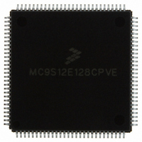
MC9S12E128CPVE Freescale Semiconductor, MC9S12E128CPVE Datasheet - Page 544

MC9S12E128CPVE
Manufacturer Part Number
MC9S12E128CPVE
Description
IC MCU 128K FLASH 25MHZ 112-LQFP
Manufacturer
Freescale Semiconductor
Series
HCS12r
Specifications of MC9S12E128CPVE
Core Processor
HCS12
Core Size
16-Bit
Speed
25MHz
Connectivity
EBI/EMI, I²C, SCI, SPI
Peripherals
POR, PWM, WDT
Number Of I /o
91
Program Memory Size
128KB (128K x 8)
Program Memory Type
FLASH
Ram Size
8K x 8
Voltage - Supply (vcc/vdd)
2.35 V ~ 2.75 V
Data Converters
A/D 16x10b; D/A 2x8b
Oscillator Type
Internal
Operating Temperature
-40°C ~ 85°C
Package / Case
112-LQFP
Processor Series
S12E
Core
HCS12
Data Bus Width
16 bit
Data Ram Size
8 KB
Interface Type
SCI/SPI
Maximum Clock Frequency
25 MHz
Number Of Programmable I/os
92
Number Of Timers
12
Operating Supply Voltage
3.135 V to 5.5 V
Maximum Operating Temperature
+ 85 C
Mounting Style
SMD/SMT
3rd Party Development Tools
EWHCS12
Minimum Operating Temperature
- 40 C
On-chip Adc
16-ch x 10-bit
On-chip Dac
2-ch x 8-bit
Controller Family/series
HCS12/S12X
No. Of I/o's
90
Ram Memory Size
8KB
Cpu Speed
25MHz
No. Of Timers
4
Embedded Interface Type
I2C, SCI, SPI
Rohs Compliant
Yes
For Use With
M68EVB912E128 - BOARD EVAL FOR MC9S12E128/64
Lead Free Status / RoHS Status
Lead free / RoHS Compliant
Eeprom Size
-
Lead Free Status / Rohs Status
Lead free / RoHS Compliant
Available stocks
Company
Part Number
Manufacturer
Quantity
Price
Company:
Part Number:
MC9S12E128CPVE
Manufacturer:
Freescale Semiconductor
Quantity:
10 000
- Current page: 544 of 606
- Download datasheet (4Mb)
Chapter 19 Module Mapping Control (MMCV4)
19.1.1
19.1.2
Some of the registers operate differently depending on the mode of operation (i.e., normal expanded wide,
special single chip, etc.). This is best understood from the register descriptions.
19.2
All interfacing with the MMC sub-block is done within the core, it has no external signals.
19.3
A summary of the registers associated with the MMC sub-block is shown in
descriptions of the registers and bits are given in the subsections that follow.
19.3.1
544
•
•
•
•
•
•
•
•
•
•
•
Registers for mapping of address space for on-chip RAM, EEPROM, and FLASH (or ROM)
memory blocks and associated registers
Memory mapping control and selection based upon address decode and system operating mode
Core address bus control
Core data bus control and multiplexing
Core security state decoding
Emulation chip select signal generation (ECS)
External chip select signal generation (XCS)
Internal memory expansion
External stretch and ROM mapping control functions via the MISC register
Reserved registers for test purposes
Configurable system memory options defined at integration of core into the system-on-a-chip
(SoC).
External Signal Description
Memory Map and Register Definition
Address
Offset
Features
Modes of Operation
Module Memory Map
.
.
Initialization of Internal RAM Position Register (INITRM)
Initialization of Internal Registers Position Register (INITRG)
Initialization of Internal EEPROM Position Register (INITEE)
Miscellaneous System Control Register (MISC)
Reserved
MC9S12E128 Data Sheet, Rev. 1.07
Table 19-1. MMC Memory Map
Register
.
.
Figure
19-2. Detailed
Freescale Semiconductor
Access
R/W
R/W
R/W
R/W
—
—
Related parts for MC9S12E128CPVE
Image
Part Number
Description
Manufacturer
Datasheet
Request
R
Part Number:
Description:
Manufacturer:
Freescale Semiconductor, Inc
Datasheet:
Part Number:
Description:
Manufacturer:
Freescale Semiconductor, Inc
Datasheet:
Part Number:
Description:
Manufacturer:
Freescale Semiconductor, Inc
Datasheet:
Part Number:
Description:
Manufacturer:
Freescale Semiconductor, Inc
Datasheet:
Part Number:
Description:
Manufacturer:
Freescale Semiconductor, Inc
Datasheet:
Part Number:
Description:
Manufacturer:
Freescale Semiconductor, Inc
Datasheet:
Part Number:
Description:
Manufacturer:
Freescale Semiconductor, Inc
Datasheet:
Part Number:
Description:
Manufacturer:
Freescale Semiconductor, Inc
Datasheet:
Part Number:
Description:
Manufacturer:
Freescale Semiconductor, Inc
Datasheet:
Part Number:
Description:
Manufacturer:
Freescale Semiconductor, Inc
Datasheet:
Part Number:
Description:
Manufacturer:
Freescale Semiconductor, Inc
Datasheet:
Part Number:
Description:
Manufacturer:
Freescale Semiconductor, Inc
Datasheet:
Part Number:
Description:
Manufacturer:
Freescale Semiconductor, Inc
Datasheet:
Part Number:
Description:
Manufacturer:
Freescale Semiconductor, Inc
Datasheet:
Part Number:
Description:
Manufacturer:
Freescale Semiconductor, Inc
Datasheet:


