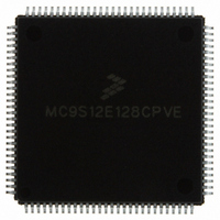
MC9S12E128CPVE Freescale Semiconductor, MC9S12E128CPVE Datasheet - Page 67

MC9S12E128CPVE
Manufacturer Part Number
MC9S12E128CPVE
Description
IC MCU 128K FLASH 25MHZ 112-LQFP
Manufacturer
Freescale Semiconductor
Series
HCS12r
Specifications of MC9S12E128CPVE
Core Processor
HCS12
Core Size
16-Bit
Speed
25MHz
Connectivity
EBI/EMI, I²C, SCI, SPI
Peripherals
POR, PWM, WDT
Number Of I /o
91
Program Memory Size
128KB (128K x 8)
Program Memory Type
FLASH
Ram Size
8K x 8
Voltage - Supply (vcc/vdd)
2.35 V ~ 2.75 V
Data Converters
A/D 16x10b; D/A 2x8b
Oscillator Type
Internal
Operating Temperature
-40°C ~ 85°C
Package / Case
112-LQFP
Processor Series
S12E
Core
HCS12
Data Bus Width
16 bit
Data Ram Size
8 KB
Interface Type
SCI/SPI
Maximum Clock Frequency
25 MHz
Number Of Programmable I/os
92
Number Of Timers
12
Operating Supply Voltage
3.135 V to 5.5 V
Maximum Operating Temperature
+ 85 C
Mounting Style
SMD/SMT
3rd Party Development Tools
EWHCS12
Minimum Operating Temperature
- 40 C
On-chip Adc
16-ch x 10-bit
On-chip Dac
2-ch x 8-bit
Controller Family/series
HCS12/S12X
No. Of I/o's
90
Ram Memory Size
8KB
Cpu Speed
25MHz
No. Of Timers
4
Embedded Interface Type
I2C, SCI, SPI
Rohs Compliant
Yes
For Use With
M68EVB912E128 - BOARD EVAL FOR MC9S12E128/64
Lead Free Status / RoHS Status
Lead free / RoHS Compliant
Eeprom Size
-
Lead Free Status / Rohs Status
Lead free / RoHS Compliant
Available stocks
Company
Part Number
Manufacturer
Quantity
Price
Company:
Part Number:
MC9S12E128CPVE
Manufacturer:
Freescale Semiconductor
Quantity:
10 000
- Current page: 67 of 606
- Download datasheet (4Mb)
programmable to either falling edge-sensitive triggering or level-sensitive triggering based on the setting
of the IRQE bit in the IRQCR register. The IRQ is always enabled and configured to level-sensitive
triggering out of reset. It can be disabled by clearing IRQEN bit in the IRQCR register. There is an active
pull-up on this pin while in reset and immediately out of reset. The pullup can be turned off by clearing
PUPEE in the PUCR register.
1.4.15
PE0 is always an input and can always be read. The PE0 pin is also the XIRQ input for requesting a
nonmaskable asynchronous interrupt to the MCU. During reset, the X bit in the condition code register
(CCR) is set and any XIRQ interrupt is masked until MCU software enables it by clearing the X bit.
Because the XIRQ input is level sensitive triggered, it can be connected to a multiple-source wired-OR
network. There is an active pull-up on this pin while in reset and immediately out of reset. The pullup can
be turned off by clearing PUPEE in the PUCR register.
1.4.16
PK7 is a general purpose input or output pin. During MCU expanded modes of operation, when the EMK
bit in the MODE register is set to 1, this pin is used as the emulation chip select output (ECS). In expanded
modes the PK7 pin can be used to determine the reset state of the ROMON bit in the MISC register. At the
rising edge of RESET, the state of the PK7 pin is latched to the ROMON bit. There is an active pull-up on
this pin while in reset and immediately out of reset. The pullup can be turned off by clearing PUPKE in
the PUCR register. Refer to the HCS12 MEBI block description chapter for further details. PK7 is not
available in the 80 pin package version.
1.4.17
PK6 is a general purpose input or output pin. During MCU expanded modes of operation, when the EMK
bit in the MODE register is set to 1, this pin is used as an external chip select signal for most external
accesses that are not selected by ECS. There is an active pull-up on this pin while in reset and immediately
out of reset. The pullup can be turned off by clearing PUPKE in the PUCR register. Refer to the HCS12
MEBI block description chapter for further details. PK6 is not available in the 80 pin package version.
1.4.18
PK[5:0] are general purpose input or output pins. In MCU expanded modes of operation, when the EMK
bit in the MODE register is set to 1, PK[5:0] provide the expanded address XADDR[19:14] for the external
bus. There are active pull-ups on PK[5:0] pins while in reset and immediately out of reset. The pullup can
be turned off by clearing PUPKE in the PUCR register. Refer to the HCS12 MEBI block description
chapter for further details. PK[5:0] are not available in the 80 pin package version.
1.4.19
PAD[15:0] are the analog inputs for the analog to digital converter (ADC). They can also be configured as
general purpose digital input or output pin. When enabled as digital inputs or outputs, the PAD[15:0] can
Freescale Semiconductor
PE0 / XIRQ — Port E input Pin 0 / Non Maskable Interrupt Pin
PK7 / ECS / ROMCTL — Port K I/O Pin 7
PK6 / XCS — Port K I/O Pin 6
PK[5:0] / XADDR[19:14] — Port K I/O Pins [5:0]
PAD[15:0] / AN[15:0] / KWAD[15:0] — Port AD I/O Pins [15:0]
MC9S12E128 Data Sheet, Rev. 1.07
Chapter 1 MC9S12E128 Device Overview (MC9S12E128DGV1)
67
Related parts for MC9S12E128CPVE
Image
Part Number
Description
Manufacturer
Datasheet
Request
R
Part Number:
Description:
Manufacturer:
Freescale Semiconductor, Inc
Datasheet:
Part Number:
Description:
Manufacturer:
Freescale Semiconductor, Inc
Datasheet:
Part Number:
Description:
Manufacturer:
Freescale Semiconductor, Inc
Datasheet:
Part Number:
Description:
Manufacturer:
Freescale Semiconductor, Inc
Datasheet:
Part Number:
Description:
Manufacturer:
Freescale Semiconductor, Inc
Datasheet:
Part Number:
Description:
Manufacturer:
Freescale Semiconductor, Inc
Datasheet:
Part Number:
Description:
Manufacturer:
Freescale Semiconductor, Inc
Datasheet:
Part Number:
Description:
Manufacturer:
Freescale Semiconductor, Inc
Datasheet:
Part Number:
Description:
Manufacturer:
Freescale Semiconductor, Inc
Datasheet:
Part Number:
Description:
Manufacturer:
Freescale Semiconductor, Inc
Datasheet:
Part Number:
Description:
Manufacturer:
Freescale Semiconductor, Inc
Datasheet:
Part Number:
Description:
Manufacturer:
Freescale Semiconductor, Inc
Datasheet:
Part Number:
Description:
Manufacturer:
Freescale Semiconductor, Inc
Datasheet:
Part Number:
Description:
Manufacturer:
Freescale Semiconductor, Inc
Datasheet:
Part Number:
Description:
Manufacturer:
Freescale Semiconductor, Inc
Datasheet:


