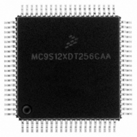
MC9S12XDT256CAA Freescale Semiconductor, MC9S12XDT256CAA Datasheet - Page 101

MC9S12XDT256CAA
Manufacturer Part Number
MC9S12XDT256CAA
Description
IC MCU 256K FLASH 80-QFP
Manufacturer
Freescale Semiconductor
Series
HCS12r
Datasheet
1.MC9S12XD64CAA.pdf
(1348 pages)
Specifications of MC9S12XDT256CAA
Core Processor
HCS12X
Core Size
16-Bit
Speed
80MHz
Connectivity
CAN, EBI/EMI, I²C, IrDA, LIN, SCI, SPI
Peripherals
LVD, POR, PWM, WDT
Number Of I /o
59
Program Memory Size
256KB (256K x 8)
Program Memory Type
FLASH
Eeprom Size
4K x 8
Ram Size
16K x 8
Voltage - Supply (vcc/vdd)
2.35 V ~ 5.5 V
Data Converters
A/D 8x10b
Oscillator Type
External
Operating Temperature
-40°C ~ 85°C
Package / Case
80-QFP
Processor Series
S12XD
Core
HCS12
Data Bus Width
16 bit
Data Ram Size
16 KB
Interface Type
CAN/I2C/SCI/SPI
Maximum Clock Frequency
40 MHz
Number Of Programmable I/os
59
Number Of Timers
12
Maximum Operating Temperature
+ 85 C
Mounting Style
SMD/SMT
3rd Party Development Tools
EWHCS12
Development Tools By Supplier
EVB9S12XDP512E
Minimum Operating Temperature
- 40 C
On-chip Adc
8-ch x 10-bit
Lead Free Status / RoHS Status
Lead free / RoHS Compliant
Available stocks
Company
Part Number
Manufacturer
Quantity
Price
Company:
Part Number:
MC9S12XDT256CAA
Manufacturer:
Freescale Semiconductor
Quantity:
10 000
Company:
Part Number:
MC9S12XDT256CAAR
Manufacturer:
Freescale Semiconductor
Quantity:
10 000
- Current page: 101 of 1348
- Download datasheet (8Mb)
The clock generator creates the clocks used in the MCU (see
top of the individual clock gates indicates the dependencies of different modes (STOP, WAIT) and the
setting of the respective configuration bits.
The peripheral modules use the bus clock. Some peripheral modules also use the oscillator clock. The
memory blocks use the bus clock. If the MCU enters self clock mode (see
Mode”) oscillator clock source is switched to PLLCLK running at its minimum frequency f
clock is used to generate the clock visible at the ECLK pin. The core clock signal is the clock for the CPU.
The core clock is twice the bus clock as shown in
one bus clock.
PLL clock mode is selected with PLLSEL bit in the CLKSEL registerr. When selected, the PLL output
clock drives SYSCLK for the main system including the CPU and peripherals. The PLL cannot be turned
off by clearing the PLLON bit, if the PLL clock is selected. When PLLSEL is changed, it takes a maximum
of 4 OSCCLK plus 4 PLLCLK cycles to make the transition. During the transition, all clocks freeze and
CPU activity ceases.
2.4.1.3
If no OSCCLK edges are detected within a certain time, the clock monitor within the oscillator block
generates a clock monitor fail event. The CRG then asserts self clock mode or generates a system reset
depending on the state of SCME bit. If the clock monitor is disabled or the presence of clocks is detected
no failure is indicated by the oscillator block.The clock monitor function is enabled/disabled by the CME
control bit.
2.4.1.4
The clock monitor performs a coarse check on the incoming clock signal. The clock quality checker
provides a more accurate check in addition to the clock monitor.
A clock quality check is triggered by any of the following events:
A time window of 50,000 VCO clock cycles
1. VCO clock cycles are generated by the PLL when running at minimum frequency f
Freescale Semiconductor
•
•
•
•
Power on reset (POR)
Low voltage reset (LVR)
Wake-up from full stop mode (exit full stop)
Clock monitor fail indication (CM fail)
BUS CLOCK / ECLK
Clock Monitor (CM)
Clock Quality Checker
CORE CLOCK
Figure 2-18. Core Clock and Bus Clock Relationship
MC9S12XDP512 Data Sheet, Rev. 2.21
1
is called check window.
Figure
2-18. But note that a CPU cycle corresponds to
Figure
Chapter 2 Clocks and Reset Generator (S12CRGV6)
2-17). The gating condition placed on
SCM
.
Section 2.4.2.2, “Self Clock
SCM
. The bus
101
Related parts for MC9S12XDT256CAA
Image
Part Number
Description
Manufacturer
Datasheet
Request
R

Part Number:
Description:
16-BIT MICROPROCESSOR FAMILY
Manufacturer:
FREESCALE [Freescale Semiconductor, Inc]
Datasheet:
Part Number:
Description:
Manufacturer:
Freescale Semiconductor, Inc
Datasheet:
Part Number:
Description:
Manufacturer:
Freescale Semiconductor, Inc
Datasheet:
Part Number:
Description:
Manufacturer:
Freescale Semiconductor, Inc
Datasheet:
Part Number:
Description:
Manufacturer:
Freescale Semiconductor, Inc
Datasheet:
Part Number:
Description:
Manufacturer:
Freescale Semiconductor, Inc
Datasheet:
Part Number:
Description:
Manufacturer:
Freescale Semiconductor, Inc
Datasheet:
Part Number:
Description:
Manufacturer:
Freescale Semiconductor, Inc
Datasheet:
Part Number:
Description:
Manufacturer:
Freescale Semiconductor, Inc
Datasheet:
Part Number:
Description:
Manufacturer:
Freescale Semiconductor, Inc
Datasheet:
Part Number:
Description:
Manufacturer:
Freescale Semiconductor, Inc
Datasheet:
Part Number:
Description:
Manufacturer:
Freescale Semiconductor, Inc
Datasheet:
Part Number:
Description:
Manufacturer:
Freescale Semiconductor, Inc
Datasheet:
Part Number:
Description:
Manufacturer:
Freescale Semiconductor, Inc
Datasheet:
Part Number:
Description:
Manufacturer:
Freescale Semiconductor, Inc
Datasheet:


