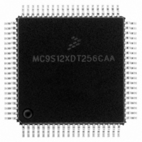
MC9S12XDT256CAA Freescale Semiconductor, MC9S12XDT256CAA Datasheet - Page 342

MC9S12XDT256CAA
Manufacturer Part Number
MC9S12XDT256CAA
Description
IC MCU 256K FLASH 80-QFP
Manufacturer
Freescale Semiconductor
Series
HCS12r
Datasheet
1.MC9S12XD64CAA.pdf
(1348 pages)
Specifications of MC9S12XDT256CAA
Core Processor
HCS12X
Core Size
16-Bit
Speed
80MHz
Connectivity
CAN, EBI/EMI, I²C, IrDA, LIN, SCI, SPI
Peripherals
LVD, POR, PWM, WDT
Number Of I /o
59
Program Memory Size
256KB (256K x 8)
Program Memory Type
FLASH
Eeprom Size
4K x 8
Ram Size
16K x 8
Voltage - Supply (vcc/vdd)
2.35 V ~ 5.5 V
Data Converters
A/D 8x10b
Oscillator Type
External
Operating Temperature
-40°C ~ 85°C
Package / Case
80-QFP
Processor Series
S12XD
Core
HCS12
Data Bus Width
16 bit
Data Ram Size
16 KB
Interface Type
CAN/I2C/SCI/SPI
Maximum Clock Frequency
40 MHz
Number Of Programmable I/os
59
Number Of Timers
12
Maximum Operating Temperature
+ 85 C
Mounting Style
SMD/SMT
3rd Party Development Tools
EWHCS12
Development Tools By Supplier
EVB9S12XDP512E
Minimum Operating Temperature
- 40 C
On-chip Adc
8-ch x 10-bit
Lead Free Status / RoHS Status
Lead free / RoHS Compliant
Available stocks
Company
Part Number
Manufacturer
Quantity
Price
Company:
Part Number:
MC9S12XDT256CAA
Manufacturer:
Freescale Semiconductor
Quantity:
10 000
Company:
Part Number:
MC9S12XDT256CAAR
Manufacturer:
Freescale Semiconductor
Quantity:
10 000
- Current page: 342 of 1348
- Download datasheet (8Mb)
Chapter 7 Enhanced Capture Timer (S12ECT16B8CV2)
7.3.2.24
Read: Anytime
Write: Once in normal modes
All bits reset to zero.
342
BUFFEN
TFMOD
PACMX
Reset
Field
SHxy
7:4
3
2
1
W
R
SH37
Share Input action of Input Capture Channels x and y
0 Normal operation
1 The channel input ‘x’ causes the same action on the channel ‘y’. The port pin ‘x’ and the corresponding edge
Timer Flag Setting Mode — Use of the TFMOD bit in conjunction with the use of the ICOVW register allows a
timer interrupt to be generated after capturing two values in the capture and holding registers instead of
generating an interrupt for every capture.
By setting TFMOD in queue mode, when NOVWx bit is set and the corresponding capture and holding registers
are emptied, an input capture event will first update the related input capture register with the main timer
contents. At the next event, the TCx data is transferred to the TCxH register, the TCx is updated and the CxF
interrupt flag is set. In all other input capture cases the interrupt flag is set by a valid external event on PTx.
0 The timer flags C3F–C0F in TFLG1 are set when a valid input capture transition on the corresponding port pin
1 If in queue mode (BUFEN = 1 and LATQ = 0), the timer flags C3F–C0F in TFLG1 are set only when a latch
8-Bit Pulse Accumulators Maximum Count
0 Normal operation. When the 8-bit pulse accumulator has reached the value 0x00FF, with the next active edge,
1 When the 8-bit pulse accumulator has reached the value 0x00FF, it will not be incremented further. The value
IC Buffer Enable
0 Input capture and pulse accumulator holding registers are disabled.
1 Input capture and pulse accumulator holding registers are enabled. The latching mode is defined by LATQ
Input Control System Control Register (ICSYS)
0
7
detector is used to be active on the channel ‘y’.
occurs.
on the corresponding holding register occurs. If the queue mode is not engaged, the timer flags C3F–C0F are
set the same way as for TFMOD = 0.
it will be incremented to 0x0000.
0x00FF indicates a count of 255 or more.
control bit.
SH26
0
6
Figure 7-46. Input Control System Register (ICSYS)
Table 7-30. ICSYS Field Descriptions
MC9S12XDP512 Data Sheet, Rev. 2.21
SH15
0
5
SH04
0
4
Description
TFMOD
0
3
PACMX
0
2
BUFEN
Freescale Semiconductor
0
1
LATQ
0
0
Related parts for MC9S12XDT256CAA
Image
Part Number
Description
Manufacturer
Datasheet
Request
R

Part Number:
Description:
16-BIT MICROPROCESSOR FAMILY
Manufacturer:
FREESCALE [Freescale Semiconductor, Inc]
Datasheet:
Part Number:
Description:
Manufacturer:
Freescale Semiconductor, Inc
Datasheet:
Part Number:
Description:
Manufacturer:
Freescale Semiconductor, Inc
Datasheet:
Part Number:
Description:
Manufacturer:
Freescale Semiconductor, Inc
Datasheet:
Part Number:
Description:
Manufacturer:
Freescale Semiconductor, Inc
Datasheet:
Part Number:
Description:
Manufacturer:
Freescale Semiconductor, Inc
Datasheet:
Part Number:
Description:
Manufacturer:
Freescale Semiconductor, Inc
Datasheet:
Part Number:
Description:
Manufacturer:
Freescale Semiconductor, Inc
Datasheet:
Part Number:
Description:
Manufacturer:
Freescale Semiconductor, Inc
Datasheet:
Part Number:
Description:
Manufacturer:
Freescale Semiconductor, Inc
Datasheet:
Part Number:
Description:
Manufacturer:
Freescale Semiconductor, Inc
Datasheet:
Part Number:
Description:
Manufacturer:
Freescale Semiconductor, Inc
Datasheet:
Part Number:
Description:
Manufacturer:
Freescale Semiconductor, Inc
Datasheet:
Part Number:
Description:
Manufacturer:
Freescale Semiconductor, Inc
Datasheet:
Part Number:
Description:
Manufacturer:
Freescale Semiconductor, Inc
Datasheet:


