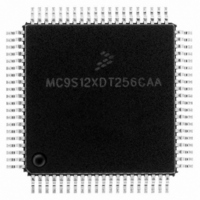
MC9S12XDT256CAA Freescale Semiconductor, MC9S12XDT256CAA Datasheet - Page 385

MC9S12XDT256CAA
Manufacturer Part Number
MC9S12XDT256CAA
Description
IC MCU 256K FLASH 80-QFP
Manufacturer
Freescale Semiconductor
Series
HCS12r
Datasheet
1.MC9S12XD64CAA.pdf
(1348 pages)
Specifications of MC9S12XDT256CAA
Core Processor
HCS12X
Core Size
16-Bit
Speed
80MHz
Connectivity
CAN, EBI/EMI, I²C, IrDA, LIN, SCI, SPI
Peripherals
LVD, POR, PWM, WDT
Number Of I /o
59
Program Memory Size
256KB (256K x 8)
Program Memory Type
FLASH
Eeprom Size
4K x 8
Ram Size
16K x 8
Voltage - Supply (vcc/vdd)
2.35 V ~ 5.5 V
Data Converters
A/D 8x10b
Oscillator Type
External
Operating Temperature
-40°C ~ 85°C
Package / Case
80-QFP
Processor Series
S12XD
Core
HCS12
Data Bus Width
16 bit
Data Ram Size
16 KB
Interface Type
CAN/I2C/SCI/SPI
Maximum Clock Frequency
40 MHz
Number Of Programmable I/os
59
Number Of Timers
12
Maximum Operating Temperature
+ 85 C
Mounting Style
SMD/SMT
3rd Party Development Tools
EWHCS12
Development Tools By Supplier
EVB9S12XDP512E
Minimum Operating Temperature
- 40 C
On-chip Adc
8-ch x 10-bit
Lead Free Status / RoHS Status
Lead free / RoHS Compliant
Available stocks
Company
Part Number
Manufacturer
Quantity
Price
Company:
Part Number:
MC9S12XDT256CAA
Manufacturer:
Freescale Semiconductor
Quantity:
10 000
Company:
Part Number:
MC9S12XDT256CAAR
Manufacturer:
Freescale Semiconductor
Quantity:
10 000
- Current page: 385 of 1348
- Download datasheet (8Mb)
On the front end of the PWM timer, the clock is enabled to the PWM circuit by the PWMEx bit being high.
There is an edge-synchronizing circuit to guarantee that the clock will only be enabled or disabled at an
edge. When the channel is disabled (PWMEx = 0), the counter for the channel does not count.
8.4.2.2
Each channel has a polarity bit to allow starting a waveform cycle with a high or low signal. This is shown
on the block diagram as a mux select of either the Q output or the Q output of the PWM output flip flop.
When one of the bits in the PWMPOL register is set, the associated PWM channel output is high at the
beginning of the waveform, then goes low when the duty count is reached. Conversely, if the polarity bit
is zero, the output starts low and then goes high when the duty count is reached.
8.4.2.3
Dedicated period and duty registers exist for each channel and are double buffered so that if they change
while the channel is enabled, the change will NOT take effect until one of the following occurs:
In this way, the output of the PWM will always be either the old waveform or the new waveform, not some
variation in between. If the channel is not enabled, then writes to the period and duty registers will go
directly to the latches as well as the buffer.
A change in duty or period can be forced into effect “immediately” by writing the new value to the duty
and/or period registers and then writing to the counter. This forces the counter to reset and the new duty
and/or period values to be latched. In addition, since the counter is readable, it is possible to know where
the count is with respect to the duty value and software can be used to make adjustments
8.4.2.4
Each channel has a dedicated 8-bit up/down counter which runs at the rate of the selected clock source (see
Section 8.4.1, “PWM Clock Select”
two registers, a duty register and a period register as shown in
matches the duty register, the output flip-flop changes state, causing the PWM waveform to also change
state. A match between the PWM counter and the period register behaves differently depending on what
output mode is selected as shown in
and
Freescale Semiconductor
•
•
•
Section 8.4.2.6, “Center Aligned
The effective period ends
The counter is written (counter resets to $00)
The channel is disabled
PWM Polarity
PWM Period and Duty
PWM Timer Counters
When forcing a new period or duty into effect immediately, an irregular
PWM cycle can occur.
Depending on the polarity bit, the duty registers will contain the count of
either the high time or the low time.
MC9S12XDP512 Data Sheet, Rev. 2.21
Figure 8-19
for the available clock sources and rates). The counter compares to
Outputs”.
and described in
NOTE
Figure
Chapter 8 Pulse-Width Modulator (S12PWM8B8CV1)
Section 8.4.2.5, “Left Aligned Outputs”
8-19. When the PWM counter
385
Related parts for MC9S12XDT256CAA
Image
Part Number
Description
Manufacturer
Datasheet
Request
R

Part Number:
Description:
16-BIT MICROPROCESSOR FAMILY
Manufacturer:
FREESCALE [Freescale Semiconductor, Inc]
Datasheet:
Part Number:
Description:
Manufacturer:
Freescale Semiconductor, Inc
Datasheet:
Part Number:
Description:
Manufacturer:
Freescale Semiconductor, Inc
Datasheet:
Part Number:
Description:
Manufacturer:
Freescale Semiconductor, Inc
Datasheet:
Part Number:
Description:
Manufacturer:
Freescale Semiconductor, Inc
Datasheet:
Part Number:
Description:
Manufacturer:
Freescale Semiconductor, Inc
Datasheet:
Part Number:
Description:
Manufacturer:
Freescale Semiconductor, Inc
Datasheet:
Part Number:
Description:
Manufacturer:
Freescale Semiconductor, Inc
Datasheet:
Part Number:
Description:
Manufacturer:
Freescale Semiconductor, Inc
Datasheet:
Part Number:
Description:
Manufacturer:
Freescale Semiconductor, Inc
Datasheet:
Part Number:
Description:
Manufacturer:
Freescale Semiconductor, Inc
Datasheet:
Part Number:
Description:
Manufacturer:
Freescale Semiconductor, Inc
Datasheet:
Part Number:
Description:
Manufacturer:
Freescale Semiconductor, Inc
Datasheet:
Part Number:
Description:
Manufacturer:
Freescale Semiconductor, Inc
Datasheet:
Part Number:
Description:
Manufacturer:
Freescale Semiconductor, Inc
Datasheet:


