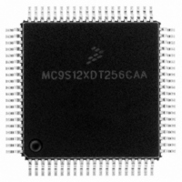
MC9S12XDT256CAA Freescale Semiconductor, MC9S12XDT256CAA Datasheet - Page 668

MC9S12XDT256CAA
Manufacturer Part Number
MC9S12XDT256CAA
Description
IC MCU 256K FLASH 80-QFP
Manufacturer
Freescale Semiconductor
Series
HCS12r
Datasheet
1.MC9S12XD64CAA.pdf
(1348 pages)
Specifications of MC9S12XDT256CAA
Core Processor
HCS12X
Core Size
16-Bit
Speed
80MHz
Connectivity
CAN, EBI/EMI, I²C, IrDA, LIN, SCI, SPI
Peripherals
LVD, POR, PWM, WDT
Number Of I /o
59
Program Memory Size
256KB (256K x 8)
Program Memory Type
FLASH
Eeprom Size
4K x 8
Ram Size
16K x 8
Voltage - Supply (vcc/vdd)
2.35 V ~ 5.5 V
Data Converters
A/D 8x10b
Oscillator Type
External
Operating Temperature
-40°C ~ 85°C
Package / Case
80-QFP
Processor Series
S12XD
Core
HCS12
Data Bus Width
16 bit
Data Ram Size
16 KB
Interface Type
CAN/I2C/SCI/SPI
Maximum Clock Frequency
40 MHz
Number Of Programmable I/os
59
Number Of Timers
12
Maximum Operating Temperature
+ 85 C
Mounting Style
SMD/SMT
3rd Party Development Tools
EWHCS12
Development Tools By Supplier
EVB9S12XDP512E
Minimum Operating Temperature
- 40 C
On-chip Adc
8-ch x 10-bit
Lead Free Status / RoHS Status
Lead free / RoHS Compliant
Available stocks
Company
Part Number
Manufacturer
Quantity
Price
Company:
Part Number:
MC9S12XDT256CAA
Manufacturer:
Freescale Semiconductor
Quantity:
10 000
Company:
Part Number:
MC9S12XDT256CAAR
Manufacturer:
Freescale Semiconductor
Quantity:
10 000
- Current page: 668 of 1348
- Download datasheet (8Mb)
Chapter 18 Memory Mapping Control (S12XMMCV3)
The fixed 16K page from 0x4000–0x7FFF (when ROMHM = 0) is the page number 0xFD.
The reset value of 0xFE ensures that there is linear Flash space available between addresses 0x4000 and
0xFFFF out of reset.
The fixed 16K page from 0xC000-0xFFFF is the page number 0xFF.
18.3.2.9
Read: Anytime
Write: Anytime
668
Address: 0x011C
PIX[7:0]
Reset
RWPE
Field
Field
AVIE
AVIF
7–0
0
1
0
Program Page Index Bits 7–0 — These page index bits are used to select which of the 256 FLASH or ROM
array pages is to be accessed in the Program Page Window.
RAM Write Protection Enable — This bit enables the RAM write protection mechanism. When the RWPE bit
is cleared, there is no write protection and any memory location is writable by the CPU module and the XGATE
module. When the RWPE bit is set the write protection mechanism is enabled and write access of the CPU or
to the XGATE RAM region. Write access performed by the XGATE module to outside of the XGATE RAM region
or the shared region is suppressed as well in this case.
0 RAM write protection check is disabled, region boundary registers can be written.
1 RAM write protection check is enabled, region boundary registers cannot be written.
CPU Access Violation Interrupt Enable — This bit enables the Access Violation Interrupt. If AVIE is set and
AVIF is set, an interrupt is generated.
0 CPU Access Violation Interrupt Disabled.
1 CPU Access Violation Interrupt Enabled.
CPU Access Violation Interrupt Flag — When set, this bit indicates that the CPU has tried to write a memory
location inside the XGATE RAM region. This flag can be reset by writing ’1’ to the AVIF bit location.
0 No access violation by the CPU was detected.
1 Access violation by the CPU was detected.
RAM Write Protection Control Register (RAMWPC)
0
7
= Unimplemented or Reserved
Figure 18-17. RAM Write Protection Control Register (RAMWPC)
0
6
Table 18-15. RAMWPC Field Descriptions
Table 18-14. PPAGE Field Descriptions
MC9S12XDP512 Data Sheet, Rev. 2.21
0
5
0
4
Description
Description
0
3
0
2
Freescale Semiconductor
0
1
0
0
Related parts for MC9S12XDT256CAA
Image
Part Number
Description
Manufacturer
Datasheet
Request
R

Part Number:
Description:
16-BIT MICROPROCESSOR FAMILY
Manufacturer:
FREESCALE [Freescale Semiconductor, Inc]
Datasheet:
Part Number:
Description:
Manufacturer:
Freescale Semiconductor, Inc
Datasheet:
Part Number:
Description:
Manufacturer:
Freescale Semiconductor, Inc
Datasheet:
Part Number:
Description:
Manufacturer:
Freescale Semiconductor, Inc
Datasheet:
Part Number:
Description:
Manufacturer:
Freescale Semiconductor, Inc
Datasheet:
Part Number:
Description:
Manufacturer:
Freescale Semiconductor, Inc
Datasheet:
Part Number:
Description:
Manufacturer:
Freescale Semiconductor, Inc
Datasheet:
Part Number:
Description:
Manufacturer:
Freescale Semiconductor, Inc
Datasheet:
Part Number:
Description:
Manufacturer:
Freescale Semiconductor, Inc
Datasheet:
Part Number:
Description:
Manufacturer:
Freescale Semiconductor, Inc
Datasheet:
Part Number:
Description:
Manufacturer:
Freescale Semiconductor, Inc
Datasheet:
Part Number:
Description:
Manufacturer:
Freescale Semiconductor, Inc
Datasheet:
Part Number:
Description:
Manufacturer:
Freescale Semiconductor, Inc
Datasheet:
Part Number:
Description:
Manufacturer:
Freescale Semiconductor, Inc
Datasheet:
Part Number:
Description:
Manufacturer:
Freescale Semiconductor, Inc
Datasheet:


