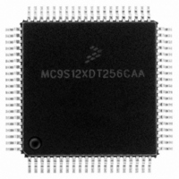
MC9S12XDT256CAA Freescale Semiconductor, MC9S12XDT256CAA Datasheet - Page 70

MC9S12XDT256CAA
Manufacturer Part Number
MC9S12XDT256CAA
Description
IC MCU 256K FLASH 80-QFP
Manufacturer
Freescale Semiconductor
Series
HCS12r
Datasheet
1.MC9S12XD64CAA.pdf
(1348 pages)
Specifications of MC9S12XDT256CAA
Core Processor
HCS12X
Core Size
16-Bit
Speed
80MHz
Connectivity
CAN, EBI/EMI, I²C, IrDA, LIN, SCI, SPI
Peripherals
LVD, POR, PWM, WDT
Number Of I /o
59
Program Memory Size
256KB (256K x 8)
Program Memory Type
FLASH
Eeprom Size
4K x 8
Ram Size
16K x 8
Voltage - Supply (vcc/vdd)
2.35 V ~ 5.5 V
Data Converters
A/D 8x10b
Oscillator Type
External
Operating Temperature
-40°C ~ 85°C
Package / Case
80-QFP
Processor Series
S12XD
Core
HCS12
Data Bus Width
16 bit
Data Ram Size
16 KB
Interface Type
CAN/I2C/SCI/SPI
Maximum Clock Frequency
40 MHz
Number Of Programmable I/os
59
Number Of Timers
12
Maximum Operating Temperature
+ 85 C
Mounting Style
SMD/SMT
3rd Party Development Tools
EWHCS12
Development Tools By Supplier
EVB9S12XDP512E
Minimum Operating Temperature
- 40 C
On-chip Adc
8-ch x 10-bit
Lead Free Status / RoHS Status
Lead free / RoHS Compliant
Available stocks
Company
Part Number
Manufacturer
Quantity
Price
Company:
Part Number:
MC9S12XDT256CAA
Manufacturer:
Freescale Semiconductor
Quantity:
10 000
Company:
Part Number:
MC9S12XDT256CAAR
Manufacturer:
Freescale Semiconductor
Quantity:
10 000
- Current page: 70 of 1348
- Download datasheet (8Mb)
Chapter 1 Device Overview MC9S12XD-Family
1
The configuration of the oscillator can be selected using the XCLKS signal (see
description please refer to the S12CRG section.
The logic level on the voltage regulator enable pin V
regulator is enabled or disabled (see
70
Normal single chip
Special single chip
Emulation single chip
Normal expanded
Emulation expanded
Special test
Internal means resources inside the MCU are read/written.
Internal Flash means Flash resources inside the MCU are read/written.
Emulation memory means resources inside the emulator are read/written (PRU registers, Flash replacement, RAM, EEPROM,
and register space are always considered internal).
External application means resources residing outside the MCU are read/written.
Chip Modes
PE7 = XCLKS
V
REGEN
0
1
1
0
BKGD =
MODC
1
0
0
1
0
0
Full swing Pierce oscillator or external clock source selected
Loop controlled Pierce oscillator selected
Internal voltage regulator enabled
Internal voltage regulator disabled, V
supplied externally
Table 1-10. Clock Selection Based on PE7
Table 1-9. Chip Modes and Data Sources
Table 1-11. Voltage Regulator VREGEN
MC9S12XDP512 Data Sheet, Rev. 2.21
Table
MODB
PE6 =
0
0
0
0
1
1
1-11).
MODA
PE5 =
0
0
1
1
1
0
REGEN
Description
Description
determines whether the on-chip voltage
ROMCTL
PK7 =
DD1,2
X
X
X
0
1
0
1
1
0
1
and V
DDPLL
EROMCTL
PE3 =
must be
X
0
1
X
X
X
0
1
X
X
Table
Freescale Semiconductor
Internal
Emulation memory
Internal Flash
External application
Internal Flash
External application
Emulation memory
Internal Flash
External application
Internal Flash
1-10). For a detailed
Data Source
1
Related parts for MC9S12XDT256CAA
Image
Part Number
Description
Manufacturer
Datasheet
Request
R

Part Number:
Description:
16-BIT MICROPROCESSOR FAMILY
Manufacturer:
FREESCALE [Freescale Semiconductor, Inc]
Datasheet:
Part Number:
Description:
Manufacturer:
Freescale Semiconductor, Inc
Datasheet:
Part Number:
Description:
Manufacturer:
Freescale Semiconductor, Inc
Datasheet:
Part Number:
Description:
Manufacturer:
Freescale Semiconductor, Inc
Datasheet:
Part Number:
Description:
Manufacturer:
Freescale Semiconductor, Inc
Datasheet:
Part Number:
Description:
Manufacturer:
Freescale Semiconductor, Inc
Datasheet:
Part Number:
Description:
Manufacturer:
Freescale Semiconductor, Inc
Datasheet:
Part Number:
Description:
Manufacturer:
Freescale Semiconductor, Inc
Datasheet:
Part Number:
Description:
Manufacturer:
Freescale Semiconductor, Inc
Datasheet:
Part Number:
Description:
Manufacturer:
Freescale Semiconductor, Inc
Datasheet:
Part Number:
Description:
Manufacturer:
Freescale Semiconductor, Inc
Datasheet:
Part Number:
Description:
Manufacturer:
Freescale Semiconductor, Inc
Datasheet:
Part Number:
Description:
Manufacturer:
Freescale Semiconductor, Inc
Datasheet:
Part Number:
Description:
Manufacturer:
Freescale Semiconductor, Inc
Datasheet:
Part Number:
Description:
Manufacturer:
Freescale Semiconductor, Inc
Datasheet:


