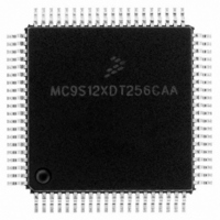
MC9S12XDT256CAA Freescale Semiconductor, MC9S12XDT256CAA Datasheet - Page 718

MC9S12XDT256CAA
Manufacturer Part Number
MC9S12XDT256CAA
Description
IC MCU 256K FLASH 80-QFP
Manufacturer
Freescale Semiconductor
Series
HCS12r
Datasheet
1.MC9S12XD64CAA.pdf
(1348 pages)
Specifications of MC9S12XDT256CAA
Core Processor
HCS12X
Core Size
16-Bit
Speed
80MHz
Connectivity
CAN, EBI/EMI, I²C, IrDA, LIN, SCI, SPI
Peripherals
LVD, POR, PWM, WDT
Number Of I /o
59
Program Memory Size
256KB (256K x 8)
Program Memory Type
FLASH
Eeprom Size
4K x 8
Ram Size
16K x 8
Voltage - Supply (vcc/vdd)
2.35 V ~ 5.5 V
Data Converters
A/D 8x10b
Oscillator Type
External
Operating Temperature
-40°C ~ 85°C
Package / Case
80-QFP
Processor Series
S12XD
Core
HCS12
Data Bus Width
16 bit
Data Ram Size
16 KB
Interface Type
CAN/I2C/SCI/SPI
Maximum Clock Frequency
40 MHz
Number Of Programmable I/os
59
Number Of Timers
12
Maximum Operating Temperature
+ 85 C
Mounting Style
SMD/SMT
3rd Party Development Tools
EWHCS12
Development Tools By Supplier
EVB9S12XDP512E
Minimum Operating Temperature
- 40 C
On-chip Adc
8-ch x 10-bit
Lead Free Status / RoHS Status
Lead free / RoHS Compliant
Available stocks
Company
Part Number
Manufacturer
Quantity
Price
Company:
Part Number:
MC9S12XDT256CAA
Manufacturer:
Freescale Semiconductor
Quantity:
10 000
Company:
Part Number:
MC9S12XDT256CAAR
Manufacturer:
Freescale Semiconductor
Quantity:
10 000
- Current page: 718 of 1348
- Download datasheet (8Mb)
Chapter 19 S12X Debug (S12XDBGV2) Module
19.4.4
The state sequence control allows a defined sequence of events to provide a trigger point for tracing of data
in the trace buffer. Once the DBG module has been armed by setting the ARM bit in the DBGC1 register,
then State1 of the state sequencer is entered. Further transitions between the states are then controlled by
the state control registers and depend upon a selected trigger mode condition being met. From final state
the only permitted transition is back to the disarmed state0. Transition between any of the states 1 to 3 is
not restricted. Each transition updates the SSF[2:0] flags in DBGSR accordingly to indicate the current
state.
Alternatively writing to the TRIG bit in DBGSC1, the final state is entered and tracing starts immediately
if the TSOURCE bits are configured for tracing.
A tag hit through TAGHI/TAGLO causes a breakpoint, if breakpoints are enabled, and ends tracing
immediately independent of the trigger alignment bits TALIGN[1:0].
Furthermore, each comparator channel can be individually configured to generate an immediate
breakpoint when a match occurs through the use of the BRK bits in the DBGxCTL registers independent
of the state sequencer state. Thus it is possible to generate an immediate breakpoint on selected channels,
while a state sequencer transition can be initiated by a match on other channels.
An XGATE S/W breakpoint request, if enabled causes a transition to the final state and generates a
breakpoint request to the CPU immediately.
If neither tracing nor breakpoints are enabled then, when a forced match triggers to final state, it can only
be returned to the disarmed state0 by clearing the ARM bit by software. This also applies to the case that
BDM breakpoints are enabled, but the BDM is disabled. Furthermore if neither tracing nor breakpoints are
enabled, forced triggers on channels with BRK set cause a transition to the state determined by the state
sequencer as if the BRK bit were not being used.
If neither tracing nor breakpoints are enabled then when a tagged match triggers to final state, the state
sequencer returns to the disarmed state0.
720
State Sequence Control
(Disarmed)
State 0
ARM=0
ARM = 0
Session complete
(disarm)
Figure 19-23. State Sequencer Diagram
ARM = 1
ARM = 0
MC9S12XDP512 Data Sheet, Rev. 2.21
Final State
State1
State3
State2
Freescale Semiconductor
Related parts for MC9S12XDT256CAA
Image
Part Number
Description
Manufacturer
Datasheet
Request
R

Part Number:
Description:
16-BIT MICROPROCESSOR FAMILY
Manufacturer:
FREESCALE [Freescale Semiconductor, Inc]
Datasheet:
Part Number:
Description:
Manufacturer:
Freescale Semiconductor, Inc
Datasheet:
Part Number:
Description:
Manufacturer:
Freescale Semiconductor, Inc
Datasheet:
Part Number:
Description:
Manufacturer:
Freescale Semiconductor, Inc
Datasheet:
Part Number:
Description:
Manufacturer:
Freescale Semiconductor, Inc
Datasheet:
Part Number:
Description:
Manufacturer:
Freescale Semiconductor, Inc
Datasheet:
Part Number:
Description:
Manufacturer:
Freescale Semiconductor, Inc
Datasheet:
Part Number:
Description:
Manufacturer:
Freescale Semiconductor, Inc
Datasheet:
Part Number:
Description:
Manufacturer:
Freescale Semiconductor, Inc
Datasheet:
Part Number:
Description:
Manufacturer:
Freescale Semiconductor, Inc
Datasheet:
Part Number:
Description:
Manufacturer:
Freescale Semiconductor, Inc
Datasheet:
Part Number:
Description:
Manufacturer:
Freescale Semiconductor, Inc
Datasheet:
Part Number:
Description:
Manufacturer:
Freescale Semiconductor, Inc
Datasheet:
Part Number:
Description:
Manufacturer:
Freescale Semiconductor, Inc
Datasheet:
Part Number:
Description:
Manufacturer:
Freescale Semiconductor, Inc
Datasheet:


