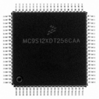
MC9S12XDT256CAA Freescale Semiconductor, MC9S12XDT256CAA Datasheet - Page 767

MC9S12XDT256CAA
Manufacturer Part Number
MC9S12XDT256CAA
Description
IC MCU 256K FLASH 80-QFP
Manufacturer
Freescale Semiconductor
Series
HCS12r
Datasheet
1.MC9S12XD64CAA.pdf
(1348 pages)
Specifications of MC9S12XDT256CAA
Core Processor
HCS12X
Core Size
16-Bit
Speed
80MHz
Connectivity
CAN, EBI/EMI, I²C, IrDA, LIN, SCI, SPI
Peripherals
LVD, POR, PWM, WDT
Number Of I /o
59
Program Memory Size
256KB (256K x 8)
Program Memory Type
FLASH
Eeprom Size
4K x 8
Ram Size
16K x 8
Voltage - Supply (vcc/vdd)
2.35 V ~ 5.5 V
Data Converters
A/D 8x10b
Oscillator Type
External
Operating Temperature
-40°C ~ 85°C
Package / Case
80-QFP
Processor Series
S12XD
Core
HCS12
Data Bus Width
16 bit
Data Ram Size
16 KB
Interface Type
CAN/I2C/SCI/SPI
Maximum Clock Frequency
40 MHz
Number Of Programmable I/os
59
Number Of Timers
12
Maximum Operating Temperature
+ 85 C
Mounting Style
SMD/SMT
3rd Party Development Tools
EWHCS12
Development Tools By Supplier
EVB9S12XDP512E
Minimum Operating Temperature
- 40 C
On-chip Adc
8-ch x 10-bit
Lead Free Status / RoHS Status
Lead free / RoHS Compliant
Available stocks
Company
Part Number
Manufacturer
Quantity
Price
Company:
Part Number:
MC9S12XDT256CAA
Manufacturer:
Freescale Semiconductor
Quantity:
10 000
Company:
Part Number:
MC9S12XDT256CAAR
Manufacturer:
Freescale Semiconductor
Quantity:
10 000
- Current page: 767 of 1348
- Download datasheet (8Mb)
The trace buffer is visible through a 2-byte window in the register address map and can be read out using
standard 16-bit word reads.
20.4.2
The S12XDBG contains four comparators, A, B, C, and D. Each comparator can be configured to monitor
either S12XCPU or XGATE buses using the SRC bit in the corresponding comparator control register.
Each comparator compares the selected address bus with the address stored in DBGXAH, DBGXAM, and
DBGXAL. Furthermore, comparators A and C also compare the data buses to the data stored in DBGXDH,
DBGXDL and allow masking of individual data bus bits.
All comparators are disabled in BDM and during BDM accesses.
The comparator match control logic (see
an exact address or an address range, whereby either an access inside or outside the specified range
generates a match condition. The comparator configuration is controlled by the control register contents
and the range control by the DBGC2 contents.
On a match a trigger can initiate a transition to another state sequencer state (see
comparator control register also allows the type of access to be included in the comparison through the use
of the RWE, RW, SZE, and SZ bits. The RWE bit controls whether read or write comparison is enabled
for the associated comparator and the RW bit selects either a read or write access for a valid match.
Similarly the SZE and SZ bits allows the size of access (word or byte) to be considered in the compare.
Only comparators B and D feature SZE and SZ.
The TAG bit in each comparator control register is used to determine the triggering condition. By setting
TAG, the comparator will qualify a match with the output of opcode tracking logic and a trigger occurs
Freescale Semiconductor
TAGHITS
EXTERNAL TAGHI / TAGLO
XGATE S/W BREAKPOINT REQUEST
SECURE
S12XCPU BUS
XGATE BUS
READ TRACE DATA (DBG READ DATA BUS)
Comparator Modes
COMPARATOR A
COMPARATOR B
COMPARATOR C
COMPARATOR D
MC9S12XDP512 Data Sheet, Rev. 2.21
Figure 20-22. S12XDBG Overview
Figure
20-22) configures comparators to monitor the buses for
MATCH0
MATCH1
MATCH2
MATCH3
CONTROL
TRIGGER
LOGIC
TAG &
Chapter 20 S12X Debug (S12XDBGV3) Module
TRIGGER
STATE
BREAKPOINT REQUESTS
S12XCPU & XGATE
Section
STATE SEQUENCER
TRACE BUFFER
TAGS
STATE
20.4.3”). The
TRACE
CONTROL
TRIGGER
769
Related parts for MC9S12XDT256CAA
Image
Part Number
Description
Manufacturer
Datasheet
Request
R

Part Number:
Description:
16-BIT MICROPROCESSOR FAMILY
Manufacturer:
FREESCALE [Freescale Semiconductor, Inc]
Datasheet:
Part Number:
Description:
Manufacturer:
Freescale Semiconductor, Inc
Datasheet:
Part Number:
Description:
Manufacturer:
Freescale Semiconductor, Inc
Datasheet:
Part Number:
Description:
Manufacturer:
Freescale Semiconductor, Inc
Datasheet:
Part Number:
Description:
Manufacturer:
Freescale Semiconductor, Inc
Datasheet:
Part Number:
Description:
Manufacturer:
Freescale Semiconductor, Inc
Datasheet:
Part Number:
Description:
Manufacturer:
Freescale Semiconductor, Inc
Datasheet:
Part Number:
Description:
Manufacturer:
Freescale Semiconductor, Inc
Datasheet:
Part Number:
Description:
Manufacturer:
Freescale Semiconductor, Inc
Datasheet:
Part Number:
Description:
Manufacturer:
Freescale Semiconductor, Inc
Datasheet:
Part Number:
Description:
Manufacturer:
Freescale Semiconductor, Inc
Datasheet:
Part Number:
Description:
Manufacturer:
Freescale Semiconductor, Inc
Datasheet:
Part Number:
Description:
Manufacturer:
Freescale Semiconductor, Inc
Datasheet:
Part Number:
Description:
Manufacturer:
Freescale Semiconductor, Inc
Datasheet:
Part Number:
Description:
Manufacturer:
Freescale Semiconductor, Inc
Datasheet:


