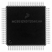
MC9S12XDT256CAA Freescale Semiconductor, MC9S12XDT256CAA Datasheet - Page 779

MC9S12XDT256CAA
Manufacturer Part Number
MC9S12XDT256CAA
Description
IC MCU 256K FLASH 80-QFP
Manufacturer
Freescale Semiconductor
Series
HCS12r
Datasheet
1.MC9S12XD64CAA.pdf
(1348 pages)
Specifications of MC9S12XDT256CAA
Core Processor
HCS12X
Core Size
16-Bit
Speed
80MHz
Connectivity
CAN, EBI/EMI, I²C, IrDA, LIN, SCI, SPI
Peripherals
LVD, POR, PWM, WDT
Number Of I /o
59
Program Memory Size
256KB (256K x 8)
Program Memory Type
FLASH
Eeprom Size
4K x 8
Ram Size
16K x 8
Voltage - Supply (vcc/vdd)
2.35 V ~ 5.5 V
Data Converters
A/D 8x10b
Oscillator Type
External
Operating Temperature
-40°C ~ 85°C
Package / Case
80-QFP
Processor Series
S12XD
Core
HCS12
Data Bus Width
16 bit
Data Ram Size
16 KB
Interface Type
CAN/I2C/SCI/SPI
Maximum Clock Frequency
40 MHz
Number Of Programmable I/os
59
Number Of Timers
12
Maximum Operating Temperature
+ 85 C
Mounting Style
SMD/SMT
3rd Party Development Tools
EWHCS12
Development Tools By Supplier
EVB9S12XDP512E
Minimum Operating Temperature
- 40 C
On-chip Adc
8-ch x 10-bit
Lead Free Status / RoHS Status
Lead free / RoHS Compliant
Available stocks
Company
Part Number
Manufacturer
Quantity
Price
Company:
Part Number:
MC9S12XDT256CAA
Manufacturer:
Freescale Semiconductor
Quantity:
10 000
Company:
Part Number:
MC9S12XDT256CAAR
Manufacturer:
Freescale Semiconductor
Quantity:
10 000
- Current page: 779 of 1348
- Download datasheet (8Mb)
20.4.5.4
The data stored in the Trace Buffer can be read using either the background debug module (BDM) module
or the S12XCPU provided the S12XDBG module is not armed, is configured for tracing (at least one
TSOURCE bit is set) and the system not secured. When the ARM bit is written to 1 the trace buffer is
locked to prevent reading. The trace buffer can only be unlocked for reading by a single aligned word write
to DBGTB when the module is disarmed. Multiple writes to the DBGTB are not allowed since they
increment the pointer.
The Trace Buffer can only be read through the DBGTB register using aligned word reads, any byte or
misaligned reads return 0 and do not cause the trace buffer pointer to increment to the next trace buffer
address. The Trace Buffer data is read out first-in first-out. By reading CNT in DBGCNT the number of
valid 64-bit lines can be determined. DBGCNT will not decrement as data is read.
Whilst reading an internal pointer is used to determine the next line to be read. After a tracing session, the
pointer points to the oldest data entry, thus if no overflow has occurred, the pointer points to line0,
otherwise it points to the line with the oldest entry. The pointer is initialized by each aligned write to
DBGTBH to point to the oldest data again. This enables an interrupted trace buffer read sequence to be
easily restarted from the oldest data entry.
Freescale Semiconductor
COCF
XOCF
XACK
Field
CRW
XRW
XSZ
5
4
3
2
1
0
Read Write Indicator — This bit indicates if the corresponding stored address corresponds to a read or write
access. This bit only contains valid information when tracing S12XCPU activity in Detail Mode.
0 Write Access
1 Read Access
S12XCPU Opcode Fetch Indicator — This bit indicates if the stored address corresponds to an opcode fetch
cycle. This bit only contains valid information when tracing the XGATE accesses in Detail Mode.
0 Stored information does not correspond to opcode fetch cycle
1 Stored information corresponds to opcode fetch cycle
XGATE Access Indicator — This bit indicates if the stored XGATE address corresponds to a free cycle. This bit
only contains valid information when tracing the S12XCPU accesses in Detail Mode.
0 Stored information corresponds to free cycle
1 Stored information does not correspond to free cycle
Access Type Indicator — This bit indicates if the access was a byte or word size access. This bit only contains
valid information when tracing XGATE activity in Detail Mode.
0 Word Access
1 Byte Access
Read Write Indicator — This bit indicates if the corresponding stored address corresponds to a read or write
access. This bit only contains valid information when tracing XGATE activity in Detail Mode.
0 Write Access
1 Read Access
XGATE Opcode Fetch Indicator — This bit indicates if the stored address corresponds to an opcode fetch
cycle.This bit only contains valid information when tracing the S12XCPU accesses in Detail Mode.
0 Stored information does not correspond to opcode fetch cycle
1 Stored information corresponds to opcode fetch cycle
Reading Data from Trace Buffer
Table 20-42. CXINF Field Descriptions (continued)
MC9S12XDP512 Data Sheet, Rev. 2.21
Description
Chapter 20 S12X Debug (S12XDBGV3) Module
781
Related parts for MC9S12XDT256CAA
Image
Part Number
Description
Manufacturer
Datasheet
Request
R

Part Number:
Description:
16-BIT MICROPROCESSOR FAMILY
Manufacturer:
FREESCALE [Freescale Semiconductor, Inc]
Datasheet:
Part Number:
Description:
Manufacturer:
Freescale Semiconductor, Inc
Datasheet:
Part Number:
Description:
Manufacturer:
Freescale Semiconductor, Inc
Datasheet:
Part Number:
Description:
Manufacturer:
Freescale Semiconductor, Inc
Datasheet:
Part Number:
Description:
Manufacturer:
Freescale Semiconductor, Inc
Datasheet:
Part Number:
Description:
Manufacturer:
Freescale Semiconductor, Inc
Datasheet:
Part Number:
Description:
Manufacturer:
Freescale Semiconductor, Inc
Datasheet:
Part Number:
Description:
Manufacturer:
Freescale Semiconductor, Inc
Datasheet:
Part Number:
Description:
Manufacturer:
Freescale Semiconductor, Inc
Datasheet:
Part Number:
Description:
Manufacturer:
Freescale Semiconductor, Inc
Datasheet:
Part Number:
Description:
Manufacturer:
Freescale Semiconductor, Inc
Datasheet:
Part Number:
Description:
Manufacturer:
Freescale Semiconductor, Inc
Datasheet:
Part Number:
Description:
Manufacturer:
Freescale Semiconductor, Inc
Datasheet:
Part Number:
Description:
Manufacturer:
Freescale Semiconductor, Inc
Datasheet:
Part Number:
Description:
Manufacturer:
Freescale Semiconductor, Inc
Datasheet:


