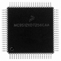
MC9S12XDT256CAA Freescale Semiconductor, MC9S12XDT256CAA Datasheet - Page 976

MC9S12XDT256CAA
Manufacturer Part Number
MC9S12XDT256CAA
Description
IC MCU 256K FLASH 80-QFP
Manufacturer
Freescale Semiconductor
Series
HCS12r
Datasheet
1.MC9S12XD64CAA.pdf
(1348 pages)
Specifications of MC9S12XDT256CAA
Core Processor
HCS12X
Core Size
16-Bit
Speed
80MHz
Connectivity
CAN, EBI/EMI, I²C, IrDA, LIN, SCI, SPI
Peripherals
LVD, POR, PWM, WDT
Number Of I /o
59
Program Memory Size
256KB (256K x 8)
Program Memory Type
FLASH
Eeprom Size
4K x 8
Ram Size
16K x 8
Voltage - Supply (vcc/vdd)
2.35 V ~ 5.5 V
Data Converters
A/D 8x10b
Oscillator Type
External
Operating Temperature
-40°C ~ 85°C
Package / Case
80-QFP
Processor Series
S12XD
Core
HCS12
Data Bus Width
16 bit
Data Ram Size
16 KB
Interface Type
CAN/I2C/SCI/SPI
Maximum Clock Frequency
40 MHz
Number Of Programmable I/os
59
Number Of Timers
12
Maximum Operating Temperature
+ 85 C
Mounting Style
SMD/SMT
3rd Party Development Tools
EWHCS12
Development Tools By Supplier
EVB9S12XDP512E
Minimum Operating Temperature
- 40 C
On-chip Adc
8-ch x 10-bit
Lead Free Status / RoHS Status
Lead free / RoHS Compliant
Available stocks
Company
Part Number
Manufacturer
Quantity
Price
Company:
Part Number:
MC9S12XDT256CAA
Manufacturer:
Freescale Semiconductor
Quantity:
10 000
Company:
Part Number:
MC9S12XDT256CAAR
Manufacturer:
Freescale Semiconductor
Quantity:
10 000
- Current page: 976 of 1348
- Download datasheet (8Mb)
Chapter 24 DG128 Port Integration Module (S12XDG128PIMV2)
External Signal Description
This section lists and describes the signals that do connect off-chip.
24.0.3
Table 24-1
“Functional Description”
978
Port
—
A
B
E
K
T
Pin Name
PB[7:0]
PE[6:5]
PE[3:2]
PK[5:0]
PT[7:0]
PA[7:0]
BKGD
shows all the pins and their functions that are controlled by the PIM. Refer to
PE[7]
PE[4]
PE[1]
PE[0]
PK[7]
Signal Properties
If there is more than one function associated with a pin, the priority is
indicated by the position in the table from top (highest priority) to bottom
(lowest priority).
Pin Function
and Priority
XCLKS
ECLKX2
IOC[7:0]
MODC
BKGD
ECLK
GPIO
GPIO
GPIO
GPIO
GPIO
GPIO
GPIO
XIRQ
GPIO
GPIO
GPIO
GPIO
IRQ
Table 24-1. Pin Functions and Priorities (Sheet 1 of 5)
for the availability of the individual pins in the different package options.
1
1
MC9S12XDP512 Data Sheet, Rev. 2.21
I/O
I/O
I/O
I/O
I/O
I/O
I/O
I/O
I/O
I/O
I/O
I/O
I/O
I/O
O
I
I
I
I
I
MODC input during RESET
S12X_BDM communication pin
General-purpose I/O
General-purpose I/O
External clock selection input during RESET
Free-running clock output at Core Clock rate (ECLK x 2)
General-purpose I/O
General-purpose I/O
Free-running clock output at the Bus Clock rate or
programmable divided in normal modes
General-purpose I/O
General-purpose I/O
Maskable level- or falling edge-sensitive interrupt input
General-purpose I/O
Non-maskable level-sensitive interrupt input
General-purpose I/O
General-purpose I/O
General-purpose I/O
Enhanced Capture Timer Channels 7–0 input/output
General-purpose I/O
NOTE
Description
Freescale Semiconductor
Section ,
Pin Function
after Reset
BKGD
GPIO
GPIO
GPIO
GPIO
Related parts for MC9S12XDT256CAA
Image
Part Number
Description
Manufacturer
Datasheet
Request
R

Part Number:
Description:
16-BIT MICROPROCESSOR FAMILY
Manufacturer:
FREESCALE [Freescale Semiconductor, Inc]
Datasheet:
Part Number:
Description:
Manufacturer:
Freescale Semiconductor, Inc
Datasheet:
Part Number:
Description:
Manufacturer:
Freescale Semiconductor, Inc
Datasheet:
Part Number:
Description:
Manufacturer:
Freescale Semiconductor, Inc
Datasheet:
Part Number:
Description:
Manufacturer:
Freescale Semiconductor, Inc
Datasheet:
Part Number:
Description:
Manufacturer:
Freescale Semiconductor, Inc
Datasheet:
Part Number:
Description:
Manufacturer:
Freescale Semiconductor, Inc
Datasheet:
Part Number:
Description:
Manufacturer:
Freescale Semiconductor, Inc
Datasheet:
Part Number:
Description:
Manufacturer:
Freescale Semiconductor, Inc
Datasheet:
Part Number:
Description:
Manufacturer:
Freescale Semiconductor, Inc
Datasheet:
Part Number:
Description:
Manufacturer:
Freescale Semiconductor, Inc
Datasheet:
Part Number:
Description:
Manufacturer:
Freescale Semiconductor, Inc
Datasheet:
Part Number:
Description:
Manufacturer:
Freescale Semiconductor, Inc
Datasheet:
Part Number:
Description:
Manufacturer:
Freescale Semiconductor, Inc
Datasheet:
Part Number:
Description:
Manufacturer:
Freescale Semiconductor, Inc
Datasheet:


