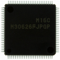
M30626FJPGP#U3C Renesas Electronics America, M30626FJPGP#U3C Datasheet - Page 208

M30626FJPGP#U3C
Manufacturer Part Number
M30626FJPGP#U3C
Description
IC M16C MCU FLASH 512K 100LQFP
Manufacturer
Renesas Electronics America
Series
M16C™ M16C/60r
Datasheets
1.QSK-62P_PLUS.pdf
(103 pages)
2.M30622SAFPU5.pdf
(308 pages)
3.M30620SPGPU3C.pdf
(423 pages)
Specifications of M30626FJPGP#U3C
Core Processor
M16C/60
Core Size
16-Bit
Speed
24MHz
Connectivity
I²C, IEBus, UART/USART
Peripherals
DMA, WDT
Number Of I /o
85
Program Memory Size
512KB (512K x 8)
Program Memory Type
FLASH
Ram Size
31K x 8
Voltage - Supply (vcc/vdd)
2.7 V ~ 5.5 V
Data Converters
A/D 26x10b; D/A 2x8b
Oscillator Type
Internal
Operating Temperature
-40°C ~ 85°C
Package / Case
100-LQFP
For Use With
867-1000 - KIT QUICK START RENESAS 62PR0K33062PS001BE - R0K33062P STARTER KITR0K33062PS000BE - KIT EVAL STARTER FOR M16C/62PM3062PT3-CPE-3 - EMULATOR COMPACT M16C/62P/30P
Lead Free Status / RoHS Status
Lead free / RoHS Compliant
Eeprom Size
-
Available stocks
Company
Part Number
Manufacturer
Quantity
Price
- Current page: 208 of 423
- Download datasheet (5Mb)
M16C/62P Group (M16C/62P, M16C/62PT)
Rev.2.41
REJ09B0185-0241
Table 17.3
Table 17.4
NOTES:
TXDi (i = 0 to 2)
(P6_3, P6_7,
P7_0)
RXDi
(P6_2, P6_6,
P7_1)
CLKi
(P6_1, P6_5,
P7_2)
CTSi/RTSi
(P6_0, P6_4,
P7_3)
P6_4
CTS1
RTS1
CTS0
CLKS1
1. In addition to this, set the CRD bit in the U0C0 register to “0” (CTS0/RTS0 enabled) and the CRS bit
2. When the CLKMD1 bit = 1 and the CLKMD0 bit = 0, the following logic levels are output:
Pin Function
Pin Name
Table 17.3 lists the functions of the input/output pins during clock synchronous serial I/O mode. Table 17.3
shows pin functions for the case where the multiple transfer clock output pin select function is deselected.
Table 17.4 lists the P6_4 Pin Functions during clock synchronous serial I/O mode. Note that for a period from
when the UARTi operating mode is selected to when transfer starts, the TXDi pin outputs an “H” (If the N-
channel open-drain output is selected, this pin is in a high-impedance state).
in the U0C0 register to “1” (RTS0 selected).
(1)
Jan 10, 2006
•High if the CLKPOL bit in the U1C0 register = 0
•Low if the CLKPOL bit = 1
Pin Functions (when not select multiple transfer clock output pin function)
P6_4 Pin Functions
Serial Data Output (Outputs dummy data when performing reception only)
Serial Data Input
Transfer Clock
Output
Transfer Clock
Input
CTS Input
RTS Output
I/O Port
Function
CRD
Page 191 of 390
U1C0 Register
1
0
0
0
−
CRS
CRD bit = 1
PD6_2 bit and PD6_6 bit in the PD6 register = 0, PD7_1 bit in the
PD7 register = 0
(Can be used as an input port when performing transmission only)
CKDIR bit in the UiMR register = 0
CKDIR bit = 1
PD6_1 bit and PD6_5 bit in the PD6 register = 0, PD7_2 bit in the
PD7 register = 0
CRD bit in the UiC0 register = 0
CRS bit in the UiC0 register = 0
PD6_0 and PD6_4 bit in the PD6 register = 0, PD7_3 bit in the PD7
register = 0
CRD bit = 0
CRS bit = 1
−
0
1
0
−
RCSP
0
0
0
1
−
Bit Set Value
UCON Register
CLKMD1
Method of Selection
1
0
0
0
0
(2)
CLKMD0
−
−
−
−
1
Input: 0, Output: 1
PD6 Register
17. Serial Interface
PD6_4
− : “0” or “1”
0
−
0
−
Related parts for M30626FJPGP#U3C
Image
Part Number
Description
Manufacturer
Datasheet
Request
R

Part Number:
Description:
KIT STARTER FOR M16C/29
Manufacturer:
Renesas Electronics America
Datasheet:

Part Number:
Description:
KIT STARTER FOR R8C/2D
Manufacturer:
Renesas Electronics America
Datasheet:

Part Number:
Description:
R0K33062P STARTER KIT
Manufacturer:
Renesas Electronics America
Datasheet:

Part Number:
Description:
KIT STARTER FOR R8C/23 E8A
Manufacturer:
Renesas Electronics America
Datasheet:

Part Number:
Description:
KIT STARTER FOR R8C/25
Manufacturer:
Renesas Electronics America
Datasheet:

Part Number:
Description:
KIT STARTER H8S2456 SHARPE DSPLY
Manufacturer:
Renesas Electronics America
Datasheet:

Part Number:
Description:
KIT STARTER FOR R8C38C
Manufacturer:
Renesas Electronics America
Datasheet:

Part Number:
Description:
KIT STARTER FOR R8C35C
Manufacturer:
Renesas Electronics America
Datasheet:

Part Number:
Description:
KIT STARTER FOR R8CL3AC+LCD APPS
Manufacturer:
Renesas Electronics America
Datasheet:

Part Number:
Description:
KIT STARTER FOR RX610
Manufacturer:
Renesas Electronics America
Datasheet:

Part Number:
Description:
KIT STARTER FOR R32C/118
Manufacturer:
Renesas Electronics America
Datasheet:

Part Number:
Description:
KIT DEV RSK-R8C/26-29
Manufacturer:
Renesas Electronics America
Datasheet:

Part Number:
Description:
KIT STARTER FOR SH7124
Manufacturer:
Renesas Electronics America
Datasheet:

Part Number:
Description:
KIT STARTER FOR H8SX/1622
Manufacturer:
Renesas Electronics America
Datasheet:

Part Number:
Description:
KIT DEV FOR SH7203
Manufacturer:
Renesas Electronics America
Datasheet:


