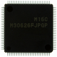
M30626FJPGP#U3C Renesas Electronics America, M30626FJPGP#U3C Datasheet - Page 82

M30626FJPGP#U3C
Manufacturer Part Number
M30626FJPGP#U3C
Description
IC M16C MCU FLASH 512K 100LQFP
Manufacturer
Renesas Electronics America
Series
M16C™ M16C/60r
Datasheets
1.QSK-62P_PLUS.pdf
(103 pages)
2.M30622SAFPU5.pdf
(308 pages)
3.M30620SPGPU3C.pdf
(423 pages)
Specifications of M30626FJPGP#U3C
Core Processor
M16C/60
Core Size
16-Bit
Speed
24MHz
Connectivity
I²C, IEBus, UART/USART
Peripherals
DMA, WDT
Number Of I /o
85
Program Memory Size
512KB (512K x 8)
Program Memory Type
FLASH
Ram Size
31K x 8
Voltage - Supply (vcc/vdd)
2.7 V ~ 5.5 V
Data Converters
A/D 26x10b; D/A 2x8b
Oscillator Type
Internal
Operating Temperature
-40°C ~ 85°C
Package / Case
100-LQFP
For Use With
867-1000 - KIT QUICK START RENESAS 62PR0K33062PS001BE - R0K33062P STARTER KITR0K33062PS000BE - KIT EVAL STARTER FOR M16C/62PM3062PT3-CPE-3 - EMULATOR COMPACT M16C/62P/30P
Lead Free Status / RoHS Status
Lead free / RoHS Compliant
Eeprom Size
-
Available stocks
Company
Part Number
Manufacturer
Quantity
Price
- Current page: 82 of 423
- Download datasheet (5Mb)
M16C/62P Group (M16C/62P, M16C/62PT)
Rev.2.41
REJ09B0185-0241
Figure 8.5
8.2.7
Table 8.5
NOTES:
8.2.8
BCLK
A0 to A19, D0 to D15, CS0 to CS3, RD, WRL,WRH,
WR, BHE
I/O ports
HLDA
Internal Peripheral Circuits
ALE Signal
1. P11 to P14 are included in the 128-pin version.
2. When I/O port function is selected.
3. The watchdog timer dose not stop when the PM22 bit in the PM2 register is set to “1” (the count
This signal is used to transfer control of the bus from the CPU or DMAC to an external circuit. When the input
on HOLD pin is pulled low, the microcomputer is placed in a hold state after the bus access then in process
finishes. The microcomputer remains in the hold state while the HOLD pin is held low, during which time the
HLDA pin outputs a low-level signal.
Table 8.5 shows the Microcomputer Status in Hold State.
Bus-using priorities are given to HOLD, DMAC, and CPU in order of decreasing precedence. However, if the
CPU is accessing an odd address in word units, the DMAC cannot gain control of the bus during two separate
accesses.
If the PM07 bit in the PM0 register is set to “0” (output enable), a clock with the same frequency as that of the
CPU clock is output as BCLK from the BCLK pin. Refer to 10.2 CPU Clock and Peripheral Function Clock.
source for the watchdog timer is the on-chip oscillator clock).
Jan 10, 2006
HOLD Signal
8.2.8 BCLK Output
Bus-Using Priorities
Microcomputer Status in Hold State
Page 65 of 390
Item
HOLD > DMAC > CPU
P0, P1, P3, P4
P6 to P14
(1)
(2)
Output
High-impedance
High-impedance
Maintains status when HOLD signal is received
Output “L”
ON (but watchdog timer stops)
Undefined
Status
(3)
8. Bus
Related parts for M30626FJPGP#U3C
Image
Part Number
Description
Manufacturer
Datasheet
Request
R

Part Number:
Description:
KIT STARTER FOR M16C/29
Manufacturer:
Renesas Electronics America
Datasheet:

Part Number:
Description:
KIT STARTER FOR R8C/2D
Manufacturer:
Renesas Electronics America
Datasheet:

Part Number:
Description:
R0K33062P STARTER KIT
Manufacturer:
Renesas Electronics America
Datasheet:

Part Number:
Description:
KIT STARTER FOR R8C/23 E8A
Manufacturer:
Renesas Electronics America
Datasheet:

Part Number:
Description:
KIT STARTER FOR R8C/25
Manufacturer:
Renesas Electronics America
Datasheet:

Part Number:
Description:
KIT STARTER H8S2456 SHARPE DSPLY
Manufacturer:
Renesas Electronics America
Datasheet:

Part Number:
Description:
KIT STARTER FOR R8C38C
Manufacturer:
Renesas Electronics America
Datasheet:

Part Number:
Description:
KIT STARTER FOR R8C35C
Manufacturer:
Renesas Electronics America
Datasheet:

Part Number:
Description:
KIT STARTER FOR R8CL3AC+LCD APPS
Manufacturer:
Renesas Electronics America
Datasheet:

Part Number:
Description:
KIT STARTER FOR RX610
Manufacturer:
Renesas Electronics America
Datasheet:

Part Number:
Description:
KIT STARTER FOR R32C/118
Manufacturer:
Renesas Electronics America
Datasheet:

Part Number:
Description:
KIT DEV RSK-R8C/26-29
Manufacturer:
Renesas Electronics America
Datasheet:

Part Number:
Description:
KIT STARTER FOR SH7124
Manufacturer:
Renesas Electronics America
Datasheet:

Part Number:
Description:
KIT STARTER FOR H8SX/1622
Manufacturer:
Renesas Electronics America
Datasheet:

Part Number:
Description:
KIT DEV FOR SH7203
Manufacturer:
Renesas Electronics America
Datasheet:


