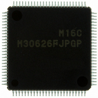
M30626FJPGP#U3C Renesas Electronics America, M30626FJPGP#U3C Datasheet - Page 95

M30626FJPGP#U3C
Manufacturer Part Number
M30626FJPGP#U3C
Description
IC M16C MCU FLASH 512K 100LQFP
Manufacturer
Renesas Electronics America
Series
M16C™ M16C/60r
Datasheets
1.QSK-62P_PLUS.pdf
(103 pages)
2.M30622SAFPU5.pdf
(308 pages)
3.M30620SPGPU3C.pdf
(423 pages)
Specifications of M30626FJPGP#U3C
Core Processor
M16C/60
Core Size
16-Bit
Speed
24MHz
Connectivity
I²C, IEBus, UART/USART
Peripherals
DMA, WDT
Number Of I /o
85
Program Memory Size
512KB (512K x 8)
Program Memory Type
FLASH
Ram Size
31K x 8
Voltage - Supply (vcc/vdd)
2.7 V ~ 5.5 V
Data Converters
A/D 26x10b; D/A 2x8b
Oscillator Type
Internal
Operating Temperature
-40°C ~ 85°C
Package / Case
100-LQFP
For Use With
867-1000 - KIT QUICK START RENESAS 62PR0K33062PS001BE - R0K33062P STARTER KITR0K33062PS000BE - KIT EVAL STARTER FOR M16C/62PM3062PT3-CPE-3 - EMULATOR COMPACT M16C/62P/30P
Lead Free Status / RoHS Status
Lead free / RoHS Compliant
Eeprom Size
-
Available stocks
Company
Part Number
Manufacturer
Quantity
Price
- Current page: 95 of 423
- Download datasheet (5Mb)
M16C/62P Group (M16C/62P, M16C/62PT)
Rev.2.41
REJ09B0185-0241
Figure 9.6
Figure 9.6 shows the External Memory Connect Example in 4-Mbyte Mode.
In this example, the CS pin of 4-Mbyte ROM is connected to the CS0 pin of microcomputer. The 4 Mbyte ROM
address input AD21, AD20 and AD19 pins are connected to the CS3, CS2 and CS1 pins of microcomputer,
respectively. The address input AD18 pin is connected to the A19 pin of microcomputer. Figures Figure 9.7 to 9.9
show the Relationship of Addresses Between the 4-Mbyte ROM and the Microcomputer for the Case of a
Connection Example in Figure 9.6.
In microprocessor mode, or in memory expansion mode where the PM13 bit in the PM1 register is “0”, banks are
located every 512 Kbytes. Setting the OFS bit in the DBR register to “1” (offset) allows the accessed address to be
offset by 40000h, so that even the data overlapping a bank boundary can be accessed in succession.
In memory expansion mode where the PM13 bit is “1,” each 512-Kbyte bank can be accessed in 256 Kbyte units
by switching them over with the OFS bit.
Because the SRAM can be accessed on condition that the chip select signals S2 = H and S1 =L, CS0 and CS2 can
be connected to S2 and S1, respectively. If the SRAM does not have the input pins to accept “H” active and “L”
active chip select signals(S1, S2), CS0 and CS2 should be decoded external to the chip.
Jan 10, 2006
External Memory Connect Example in 4-Mbyte Mode
Page 78 of 390
NOTES:
1. If only one chip select pin (S1 or S2) is present,
A0 to A16
D0 to D7
decoding by use of an external circuit is required.
CS1
CS2
CS3
CS0
A17
A19
WR
RD
17
8
DQ0 to DQ7
AD0 to AD16
AD17
AD18
AD19
AD20
AD21
OE
CS
DQ0 to DQ7
AD0 to AD16
OE
S2
S1
W
(1)
9. Memory Space Expansion Function
Related parts for M30626FJPGP#U3C
Image
Part Number
Description
Manufacturer
Datasheet
Request
R

Part Number:
Description:
KIT STARTER FOR M16C/29
Manufacturer:
Renesas Electronics America
Datasheet:

Part Number:
Description:
KIT STARTER FOR R8C/2D
Manufacturer:
Renesas Electronics America
Datasheet:

Part Number:
Description:
R0K33062P STARTER KIT
Manufacturer:
Renesas Electronics America
Datasheet:

Part Number:
Description:
KIT STARTER FOR R8C/23 E8A
Manufacturer:
Renesas Electronics America
Datasheet:

Part Number:
Description:
KIT STARTER FOR R8C/25
Manufacturer:
Renesas Electronics America
Datasheet:

Part Number:
Description:
KIT STARTER H8S2456 SHARPE DSPLY
Manufacturer:
Renesas Electronics America
Datasheet:

Part Number:
Description:
KIT STARTER FOR R8C38C
Manufacturer:
Renesas Electronics America
Datasheet:

Part Number:
Description:
KIT STARTER FOR R8C35C
Manufacturer:
Renesas Electronics America
Datasheet:

Part Number:
Description:
KIT STARTER FOR R8CL3AC+LCD APPS
Manufacturer:
Renesas Electronics America
Datasheet:

Part Number:
Description:
KIT STARTER FOR RX610
Manufacturer:
Renesas Electronics America
Datasheet:

Part Number:
Description:
KIT STARTER FOR R32C/118
Manufacturer:
Renesas Electronics America
Datasheet:

Part Number:
Description:
KIT DEV RSK-R8C/26-29
Manufacturer:
Renesas Electronics America
Datasheet:

Part Number:
Description:
KIT STARTER FOR SH7124
Manufacturer:
Renesas Electronics America
Datasheet:

Part Number:
Description:
KIT STARTER FOR H8SX/1622
Manufacturer:
Renesas Electronics America
Datasheet:

Part Number:
Description:
KIT DEV FOR SH7203
Manufacturer:
Renesas Electronics America
Datasheet:


