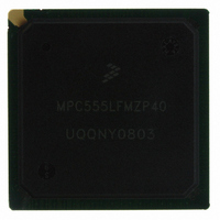
MPC555LFMZP40 Freescale Semiconductor, MPC555LFMZP40 Datasheet - Page 420

MPC555LFMZP40
Manufacturer Part Number
MPC555LFMZP40
Description
IC MCU 32BIT 40MHZ 272-BGA
Manufacturer
Freescale Semiconductor
Series
MPC5xxr
Datasheets
1.MPC555LFMZP40.pdf
(12 pages)
2.MPC555LFMZP40.pdf
(966 pages)
3.MPC555LFMZP40.pdf
(3 pages)
Specifications of MPC555LFMZP40
Core Processor
PowerPC
Core Size
32-Bit
Speed
40MHz
Connectivity
CAN, EBI/EMI, SCI, SPI, UART/USART
Peripherals
POR, PWM, WDT
Number Of I /o
101
Program Memory Size
448KB (448K x 8)
Program Memory Type
FLASH
Ram Size
26K x 8
Voltage - Supply (vcc/vdd)
2.5 V ~ 2.7 V
Data Converters
A/D 32x10b
Oscillator Type
External
Operating Temperature
-40°C ~ 125°C
Package / Case
272-PBGA
Controller Family/series
POWER 5xx
Ram Memory Size
26KB
Cpu Speed
63MIPS
Embedded Interface Type
QSPI, SCI, TouCAN
Operating Temperature Range
-40°C To +125°C
No. Of Pins
272
Rohs Compliant
No
Processor Series
MPC5xx
Core
PowerPC
Data Bus Width
32 bit
Data Ram Size
26 KB
Interface Type
CAN, QSPI, SCI
Maximum Clock Frequency
40 MHz
Number Of Programmable I/os
101
Operating Supply Voltage
3.3 V to 5 V
Maximum Operating Temperature
+ 125 C
Mounting Style
SMD/SMT
Development Tools By Supplier
MPC555CMEE
Minimum Operating Temperature
- 85 C
On-chip Adc
10 bit, 32 Channel
Cpu Family
MPC55xx
Device Core
PowerPC
Device Core Size
32b
Frequency (max)
40MHz
Total Internal Ram Size
32KB
# I/os (max)
101
Operating Supply Voltage (typ)
5V
Instruction Set Architecture
RISC
Operating Temp Range
-40C to 85C
Operating Temperature Classification
Industrial
Mounting
Surface Mount
Pin Count
272
Package Type
BGA
For Use With
MPC555CMEE - KIT EVAL FOR MPC555
Lead Free Status / RoHS Status
Contains lead / RoHS non-compliant
Eeprom Size
-
Lead Free Status / Rohs Status
No
Available stocks
Company
Part Number
Manufacturer
Quantity
Price
Company:
Part Number:
MPC555LFMZP40
Manufacturer:
MOTOLOLA
Quantity:
853
Company:
Part Number:
MPC555LFMZP40
Manufacturer:
Freescale Semiconductor
Quantity:
10 000
Company:
Part Number:
MPC555LFMZP40R2
Manufacturer:
Freescale Semiconductor
Quantity:
10 000
- Current page: 420 of 966
- Download datasheet (15Mb)
13.6.1 Port Data Register
13.6.2 Port Data Direction Register
MPC555
USER’S MANUAL
current effect of mid-level signals on the inputs used for analog signals. Digital input
signals must meet the input low voltage (VIL) or input high voltage (VIH) specifications.
If an analog input pin does not meet the digital input pin specifications when a digital
port read operation occurs, an indeterminate state is read. To avoid reading inappro-
priate values on analog inputs, the user software should employ a “masking” opera-
tion.
During a port data register read, the actual value of the pin is reported when its corre-
sponding bit in the data direction register defines the pin to be an input (port A only).
When the data direction bit specifies the pin to be an output, the content of the port
data register is read. By reading the latch which drives the output pin, software instruc-
tions that read data, modify it, and write the result, like bit manipulation instructions,
work correctly.
There is one special case to consider for digital I/O port operation. When the MUX (ex-
ternally multiplexed) bit is set in QACR0, the data direction register settings are ig-
nored for the bits corresponding to PQA[2:0], the three multiplexed address MA[2:0]
output pins. The MA[2:0] pins are forced to be digital outputs, regardless of the data
direction setting, and the multiplexed address outputs are driven. The data returned
during a port data register read is the value of the multiplexed address latches which
drive MA[2:0], regardless of the data direction setting.
QADC64 ports A and B are accessed through two 8-bit port data registers (PORTQA
and PORTQB). Port A pins are referred to as PQA when used as an 8-bit input/output
port. Port A can also be used for analog inputs AN[59:52] and external multiplexer ad-
dress outputs MA[2:0].
Port B pins are referred to as PQB when used as an 8-bit input-only digital port. Port
B can also be used for non-multiplexed AN[51:48]/AN[3:0] and multiplexed ANz, ANy,
ANx, ANw analog inputs.
PORTQA and PORTQB are unaffected by reset. Refer to
ister
The port data direction register (DDRQA) is associated with the port A digital I/O pins.
These bi-directional pins may have somewhat higher leakage and capacitance speci-
fications.
Any bit in this register set to one configures the corresponding pin as an output. Any
bit in this register cleared to zero configures the corresponding pin as an input. Soft-
ware is responsible for ensuring that DDRQA bits are not set to one on pins used for
analog inputs. When a DDRQA bit is set to one and the pin is selected for analog con-
version, the voltage sampled is that of the output digital driver as influenced by the
load.
/
for register and bit descriptions.
MPC556 QUEUED ANALOG-TO-DIGITAL CONVERTER MODULE-64
Freescale Semiconductor, Inc.
For More Information On This Product,
Go to: www.freescale.com
Rev. 15 October 2000
NOTE
13.12.4 Port A/B Data Reg-
MOTOROLA
13-8
Related parts for MPC555LFMZP40
Image
Part Number
Description
Manufacturer
Datasheet
Request
R
Part Number:
Description:
Manufacturer:
Freescale Semiconductor, Inc
Datasheet:
Part Number:
Description:
Manufacturer:
Freescale Semiconductor, Inc
Datasheet:
Part Number:
Description:
Manufacturer:
Freescale Semiconductor, Inc
Datasheet:
Part Number:
Description:
Manufacturer:
Freescale Semiconductor, Inc
Datasheet:
Part Number:
Description:
Manufacturer:
Freescale Semiconductor, Inc
Datasheet:
Part Number:
Description:
Manufacturer:
Freescale Semiconductor, Inc
Datasheet:
Part Number:
Description:
Manufacturer:
Freescale Semiconductor, Inc
Datasheet:
Part Number:
Description:
Manufacturer:
Freescale Semiconductor, Inc
Datasheet:
Part Number:
Description:
Manufacturer:
Freescale Semiconductor, Inc
Datasheet:
Part Number:
Description:
Manufacturer:
Freescale Semiconductor, Inc
Datasheet:
Part Number:
Description:
Manufacturer:
Freescale Semiconductor, Inc
Datasheet:
Part Number:
Description:
Manufacturer:
Freescale Semiconductor, Inc
Datasheet:
Part Number:
Description:
Manufacturer:
Freescale Semiconductor, Inc
Datasheet:
Part Number:
Description:
Manufacturer:
Freescale Semiconductor, Inc
Datasheet:
Part Number:
Description:
Manufacturer:
Freescale Semiconductor, Inc
Datasheet:


