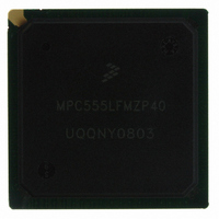
MPC555LFMZP40 Freescale Semiconductor, MPC555LFMZP40 Datasheet - Page 500

MPC555LFMZP40
Manufacturer Part Number
MPC555LFMZP40
Description
IC MCU 32BIT 40MHZ 272-BGA
Manufacturer
Freescale Semiconductor
Series
MPC5xxr
Datasheets
1.MPC555LFMZP40.pdf
(12 pages)
2.MPC555LFMZP40.pdf
(966 pages)
3.MPC555LFMZP40.pdf
(3 pages)
Specifications of MPC555LFMZP40
Core Processor
PowerPC
Core Size
32-Bit
Speed
40MHz
Connectivity
CAN, EBI/EMI, SCI, SPI, UART/USART
Peripherals
POR, PWM, WDT
Number Of I /o
101
Program Memory Size
448KB (448K x 8)
Program Memory Type
FLASH
Ram Size
26K x 8
Voltage - Supply (vcc/vdd)
2.5 V ~ 2.7 V
Data Converters
A/D 32x10b
Oscillator Type
External
Operating Temperature
-40°C ~ 125°C
Package / Case
272-PBGA
Controller Family/series
POWER 5xx
Ram Memory Size
26KB
Cpu Speed
63MIPS
Embedded Interface Type
QSPI, SCI, TouCAN
Operating Temperature Range
-40°C To +125°C
No. Of Pins
272
Rohs Compliant
No
Processor Series
MPC5xx
Core
PowerPC
Data Bus Width
32 bit
Data Ram Size
26 KB
Interface Type
CAN, QSPI, SCI
Maximum Clock Frequency
40 MHz
Number Of Programmable I/os
101
Operating Supply Voltage
3.3 V to 5 V
Maximum Operating Temperature
+ 125 C
Mounting Style
SMD/SMT
Development Tools By Supplier
MPC555CMEE
Minimum Operating Temperature
- 85 C
On-chip Adc
10 bit, 32 Channel
Cpu Family
MPC55xx
Device Core
PowerPC
Device Core Size
32b
Frequency (max)
40MHz
Total Internal Ram Size
32KB
# I/os (max)
101
Operating Supply Voltage (typ)
5V
Instruction Set Architecture
RISC
Operating Temp Range
-40C to 85C
Operating Temperature Classification
Industrial
Mounting
Surface Mount
Pin Count
272
Package Type
BGA
For Use With
MPC555CMEE - KIT EVAL FOR MPC555
Lead Free Status / RoHS Status
Contains lead / RoHS non-compliant
Eeprom Size
-
Lead Free Status / Rohs Status
No
Available stocks
Company
Part Number
Manufacturer
Quantity
Price
Company:
Part Number:
MPC555LFMZP40
Manufacturer:
MOTOLOLA
Quantity:
853
Company:
Part Number:
MPC555LFMZP40
Manufacturer:
Freescale Semiconductor
Quantity:
10 000
Company:
Part Number:
MPC555LFMZP40R2
Manufacturer:
Freescale Semiconductor
Quantity:
10 000
- Current page: 500 of 966
- Download datasheet (15Mb)
MPC555
USER’S MANUAL
After pins are assigned and configured, write data to be transmitted into transmit RAM.
Command RAM is not used in slave mode, and does not need to be initialized. Set the
queue pointers, as appropriate.
When SPE is set and MSTR is clear, a low state on the slave select PCS[0]/SS pin
begins slave mode operation at the address indicated by NEWQP. Data that is re-
ceived is stored at the pointer address in receive RAM. Data is simultaneously loaded
into the data serializer from the pointer address in transmit RAM and transmitted.
Transfer is synchronized with the externally generated SCK. The CPHA and CPOL
bits determine upon which SCK edge to latch incoming data from the MISO pin and to
drive outgoing data from the MOSI pin.
Because the command RAM is not used in slave mode, the CONT, BITSE, DT, DSCK,
and peripheral chip-select bits have no effect. The PCS[0]/SS pin is used only as an
input.
The SPBR, DT and DSCKL fields in SPCR0 and SPCR1 bits are not used in slave
mode. The QSPI drives neither the clock nor the chip-select pins and thus cannot con-
trol clock rate or transfer delay.
Because the BITSE option is not available in slave mode, the BITS field in SPCR0
specifies the number of bits to be transferred for all transfers in the queue. When the
number of bits designated by BITS[3:0] has been transferred, the QSPI stores the
working queue pointer value in CPTQP, increments the working queue pointer, and
loads new transmit data from transmit RAM into the data serializer. The working queue
pointer address is used the next time PCS[0]/SS is asserted, unless the RCPU writes
to NEWQP first.
The QSPI shifts one bit for each pulse of SCK until the slave select input goes high. If
SS goes high before the number of bits specified by the BITS field is transferred, the
QSPI resumes operation at the same pointer address the next time SS is asserted.
The maximum value that the BITS field can have is 16. If more than 16 bits are trans-
mitted before SS is negated, pointers are incremented and operation continues.
The QSPI transmits as many bits as it receives at each queue address, until the BITS
value is reached or SS is negated. SS does not need to go high between transfers as
the QSPI transfers data until reaching the end of the queue, whether SS remains low
or is toggled between transfers.
When the QSPI reaches the end of the queue, it sets the SPIF flag. If the SPIFIE bit
in SPCR2 is set, an interrupt request is generated when SPIF is asserted. At this point,
the QSPI clears SPE and stops unless wraparound mode is enabled.
Slave wraparound mode is enabled by setting the WREN bit in SPCR2. The queue can
wrap to pointer address 0x0 or to the address pointed to by NEWQP, depending on
the state of the WRTO bit in SPCR2. Slave wraparound operation is identical to master
wraparound operation.
/
MPC556
Freescale Semiconductor, Inc.
QUEUED SERIAL MULTI-CHANNEL MODULE
For More Information On This Product,
Go to: www.freescale.com
Rev. 15 October 2000
MOTOROLA
14-38
Related parts for MPC555LFMZP40
Image
Part Number
Description
Manufacturer
Datasheet
Request
R
Part Number:
Description:
Manufacturer:
Freescale Semiconductor, Inc
Datasheet:
Part Number:
Description:
Manufacturer:
Freescale Semiconductor, Inc
Datasheet:
Part Number:
Description:
Manufacturer:
Freescale Semiconductor, Inc
Datasheet:
Part Number:
Description:
Manufacturer:
Freescale Semiconductor, Inc
Datasheet:
Part Number:
Description:
Manufacturer:
Freescale Semiconductor, Inc
Datasheet:
Part Number:
Description:
Manufacturer:
Freescale Semiconductor, Inc
Datasheet:
Part Number:
Description:
Manufacturer:
Freescale Semiconductor, Inc
Datasheet:
Part Number:
Description:
Manufacturer:
Freescale Semiconductor, Inc
Datasheet:
Part Number:
Description:
Manufacturer:
Freescale Semiconductor, Inc
Datasheet:
Part Number:
Description:
Manufacturer:
Freescale Semiconductor, Inc
Datasheet:
Part Number:
Description:
Manufacturer:
Freescale Semiconductor, Inc
Datasheet:
Part Number:
Description:
Manufacturer:
Freescale Semiconductor, Inc
Datasheet:
Part Number:
Description:
Manufacturer:
Freescale Semiconductor, Inc
Datasheet:
Part Number:
Description:
Manufacturer:
Freescale Semiconductor, Inc
Datasheet:
Part Number:
Description:
Manufacturer:
Freescale Semiconductor, Inc
Datasheet:


