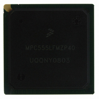
MPC555LFMZP40 Freescale Semiconductor, MPC555LFMZP40 Datasheet - Page 865

MPC555LFMZP40
Manufacturer Part Number
MPC555LFMZP40
Description
IC MCU 32BIT 40MHZ 272-BGA
Manufacturer
Freescale Semiconductor
Series
MPC5xxr
Datasheets
1.MPC555LFMZP40.pdf
(12 pages)
2.MPC555LFMZP40.pdf
(966 pages)
3.MPC555LFMZP40.pdf
(3 pages)
Specifications of MPC555LFMZP40
Core Processor
PowerPC
Core Size
32-Bit
Speed
40MHz
Connectivity
CAN, EBI/EMI, SCI, SPI, UART/USART
Peripherals
POR, PWM, WDT
Number Of I /o
101
Program Memory Size
448KB (448K x 8)
Program Memory Type
FLASH
Ram Size
26K x 8
Voltage - Supply (vcc/vdd)
2.5 V ~ 2.7 V
Data Converters
A/D 32x10b
Oscillator Type
External
Operating Temperature
-40°C ~ 125°C
Package / Case
272-PBGA
Controller Family/series
POWER 5xx
Ram Memory Size
26KB
Cpu Speed
63MIPS
Embedded Interface Type
QSPI, SCI, TouCAN
Operating Temperature Range
-40°C To +125°C
No. Of Pins
272
Rohs Compliant
No
Processor Series
MPC5xx
Core
PowerPC
Data Bus Width
32 bit
Data Ram Size
26 KB
Interface Type
CAN, QSPI, SCI
Maximum Clock Frequency
40 MHz
Number Of Programmable I/os
101
Operating Supply Voltage
3.3 V to 5 V
Maximum Operating Temperature
+ 125 C
Mounting Style
SMD/SMT
Development Tools By Supplier
MPC555CMEE
Minimum Operating Temperature
- 85 C
On-chip Adc
10 bit, 32 Channel
Cpu Family
MPC55xx
Device Core
PowerPC
Device Core Size
32b
Frequency (max)
40MHz
Total Internal Ram Size
32KB
# I/os (max)
101
Operating Supply Voltage (typ)
5V
Instruction Set Architecture
RISC
Operating Temp Range
-40C to 85C
Operating Temperature Classification
Industrial
Mounting
Surface Mount
Pin Count
272
Package Type
BGA
For Use With
MPC555CMEE - KIT EVAL FOR MPC555
Lead Free Status / RoHS Status
Contains lead / RoHS non-compliant
Eeprom Size
-
Lead Free Status / Rohs Status
No
Available stocks
Company
Part Number
Manufacturer
Quantity
Price
Company:
Part Number:
MPC555LFMZP40
Manufacturer:
MOTOLOLA
Quantity:
853
Company:
Part Number:
MPC555LFMZP40
Manufacturer:
Freescale Semiconductor
Quantity:
10 000
Company:
Part Number:
MPC555LFMZP40R2
Manufacturer:
Freescale Semiconductor
Quantity:
10 000
- Current page: 865 of 966
- Download datasheet (15Mb)
D.19.2 Host CPU Initialization of the SIOP Function
D.19.3 SIOP Function Performance
MPC555 / MPC556
USER’S MANUAL
by the value of BIT_D. In output only mode, zero will be shifted into SIOP_DATA and
in input only mode, the data shifted out is ignored. In clock-only mode SIOP_DATA is
still shifted. Note that no ‘justifying’ of SIOP_DATA is performed by the TPU, (e.g., if
an 8-bit bi-directional transfer is made, shifting lsb first, then the bottom byte of
SIOP_DATA will be shifted out and the input data will be shifted into the upper byte of
SIOP_DATA).
The CPU initializes the SIOP function by:
The TPU then starts the data transfer, and issues an interrupt request when the trans-
fer is complete.
Once the function has been initialized, the CPU only needs to write SIOP_DATA with
the new data and issue a HSR 0b11 to initiate a new transfer. In input or clock-only
modes, just the HSR 0b11 is required.
Like all TPU functions, the performance limit of the SIOP function in a given application
is dependent to some extent on the service time (latency) associated with other active
TPU channels. This is due to the operational nature of the scheduler. Where two
channels are being used for a uni-directional system, and no other TPU channels are
active, the maximum baud rate is approximately 230 KHz at a bus speed of 16.77
MHz. A three-channel bi-directional system under the same conditions has a maxi-
mum baud rate of approximately 200 KHz. When more TPU channels are active,
these performance figures will be degraded, however, the scheduler assures that the
worst case latency in any TPU application can be closely approximated. It is recom-
mended that the guidelines given in the TPU reference manual be used along with the
information given in the SIOP state timing table to perform an analysis on any pro-
posed TPU application that appears to approach the performance limits of the TPU.
1. Disabling the channel by clearing the two channel priority bits
2. Selecting the SIOP function on the channel by writing the assigned SIOP func-
3. Writing CHAN_CONTROL in the clock channel parameter RAM
4. Writing HALF_PERIOD, BIT_D and XFER_SIZE in the clock channel parame-
5. Writing SIOP_DATA if the data output is to be used
6. Selecting the required operating mode via the two host sequence bits
7. Issuing a host service request type 0b11
8. Enabling service by assigning H, M or L priority to the clock channel via the two
tion number to the function select bits
ter RAM to determine the speed, shift direction and size of the transfer
channel priority bits
SIOP_DATA is not buffered. The CPU should only access it between
completion of one transfer and the start of the next.
Freescale Semiconductor, Inc.
For More Information On This Product,
Go to: www.freescale.com
TPU ROM FUNCTIONS
Rev. 15 October 2000
NOTE
MOTOROLA
D-51
Related parts for MPC555LFMZP40
Image
Part Number
Description
Manufacturer
Datasheet
Request
R
Part Number:
Description:
Manufacturer:
Freescale Semiconductor, Inc
Datasheet:
Part Number:
Description:
Manufacturer:
Freescale Semiconductor, Inc
Datasheet:
Part Number:
Description:
Manufacturer:
Freescale Semiconductor, Inc
Datasheet:
Part Number:
Description:
Manufacturer:
Freescale Semiconductor, Inc
Datasheet:
Part Number:
Description:
Manufacturer:
Freescale Semiconductor, Inc
Datasheet:
Part Number:
Description:
Manufacturer:
Freescale Semiconductor, Inc
Datasheet:
Part Number:
Description:
Manufacturer:
Freescale Semiconductor, Inc
Datasheet:
Part Number:
Description:
Manufacturer:
Freescale Semiconductor, Inc
Datasheet:
Part Number:
Description:
Manufacturer:
Freescale Semiconductor, Inc
Datasheet:
Part Number:
Description:
Manufacturer:
Freescale Semiconductor, Inc
Datasheet:
Part Number:
Description:
Manufacturer:
Freescale Semiconductor, Inc
Datasheet:
Part Number:
Description:
Manufacturer:
Freescale Semiconductor, Inc
Datasheet:
Part Number:
Description:
Manufacturer:
Freescale Semiconductor, Inc
Datasheet:
Part Number:
Description:
Manufacturer:
Freescale Semiconductor, Inc
Datasheet:
Part Number:
Description:
Manufacturer:
Freescale Semiconductor, Inc
Datasheet:


