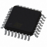
ST72F32AK2T6 STMicroelectronics, ST72F32AK2T6 Datasheet - Page 23

ST72F32AK2T6
Manufacturer Part Number
ST72F32AK2T6
Description
MCU 8BIT 8KB FLASH/ROM 32-TQFP
Manufacturer
STMicroelectronics
Series
ST7r
Datasheet
1.ST72F32AK2T6.pdf
(157 pages)
Specifications of ST72F32AK2T6
Core Processor
ST7
Core Size
8-Bit
Speed
8MHz
Connectivity
SCI, SPI
Peripherals
POR, PWM, WDT
Number Of I /o
24
Program Memory Size
8KB (8K x 8)
Program Memory Type
FLASH
Ram Size
384 x 8
Voltage - Supply (vcc/vdd)
3.8 V ~ 5.5 V
Data Converters
A/D 12x10b
Oscillator Type
External
Operating Temperature
-40°C ~ 85°C
Package / Case
32-TQFP, 32-VQFP
Processor Series
ST72F3x
Core
ST7
Data Bus Width
8 bit
Data Ram Size
384 B
Interface Type
SCI, SPI
Maximum Clock Frequency
8 MHz
Number Of Programmable I/os
32
Number Of Timers
3
Maximum Operating Temperature
+ 85 C
Mounting Style
SMD/SMT
Development Tools By Supplier
ST7232X-EVAL, ST7MDT20-DVP3, ST7MDT20J-EMU3, STX-RLINK
Minimum Operating Temperature
- 40 C
On-chip Adc
10 bit, 12 Channel
A/d Bit Size
10 bit
A/d Channels Available
12
Height
1.4 mm
Length
7 mm
Supply Voltage (max)
5.5 V
Supply Voltage (min)
3.8 V
Width
7 mm
For Use With
497-5046 - KIT TOOL FOR ST7/UPSD/STR7 MCU
Lead Free Status / RoHS Status
Lead free / RoHS Compliant
Eeprom Size
-
Lead Free Status / Rohs Status
Details
Other names
497-5610
Available stocks
Company
Part Number
Manufacturer
Quantity
Price
Company:
Part Number:
ST72F32AK2T6
Manufacturer:
STMicroelectronics
Quantity:
10 000
6 SUPPLY, RESET AND CLOCK MANAGEMENT
The device includes a range of utility features for
securing the application in critical situations (for
example in case of a power brown-out), and re-
ducing the number of external components. An
overview is shown in
For more details, refer to dedicated parametric
section.
Main features
■
■
■
6.1 PHASE LOCKED LOOP
If the clock frequency input to the PLL is in the
range 2 to 4 MHz, the PLL can be used to multiply
Figure 11. Clock, Reset and Supply Block Diagram
– 5 Crystal/Ceramic resonator oscillators
Optional PLL for multiplying the frequency by 2
Reset Sequence Manager (RSM)
Multi-Oscillator Clock Management (MO)
RESET
OSC2
OSC1
V
V
SS
DD
Figure
OSCILLATOR
RESET SEQUENCE
MULTI-
(MO)
MANAGER
(RSM)
11.
f
OSC
(option)
PLL
SICSR
SYSTEM INTEGRITY MANAGEMENT
0
the frequency by two to obtain an f
MHz. The PLL is enabled by option byte. If the PLL
is disabled, then f
Caution: The PLL is not recommended for appli-
cations where timing accuracy is required.
Figure 10. PLL Block Diagram
f
OSC
0
PLL x 2
0
/ 2
OSC2 =
0
WDG
f
RF
OSC2
f
OSC
PLL OPTION BIT
/2.
CLOCK (MCC/RTC)
WITH REALTIME
0
1
TIMER (WDG)
CONTROLLER
MAIN CLOCK
WATCHDOG
OSC2
ST7232A
f
OSC2
of 4 to 8
23/157
f
CPU
1


