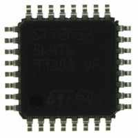
ST72F325K4T6 STMicroelectronics, ST72F325K4T6 Datasheet - Page 109

ST72F325K4T6
Manufacturer Part Number
ST72F325K4T6
Description
MCU 8BIT 16KB FLASH/ROM 32-LQFP
Manufacturer
STMicroelectronics
Series
ST7r
Datasheet
1.ST72F325K6T6.pdf
(197 pages)
Specifications of ST72F325K4T6
Core Processor
ST7
Core Size
8-Bit
Speed
8MHz
Connectivity
I²C, SCI, SPI
Peripherals
LVD, POR, PWM, WDT
Number Of I /o
24
Program Memory Size
16KB (16K x 8)
Program Memory Type
FLASH
Ram Size
512 x 8
Voltage - Supply (vcc/vdd)
3.8 V ~ 5.5 V
Data Converters
A/D 16x10b
Oscillator Type
Internal
Operating Temperature
-40°C ~ 85°C
Package / Case
32-LQFP
Processor Series
ST72F3x
Core
ST7
Data Bus Width
8 bit
Data Ram Size
512 B
Interface Type
I2C, SCI, SPI
Maximum Clock Frequency
8 MHz
Number Of Programmable I/os
48
Number Of Timers
2
Maximum Operating Temperature
+ 85 C
Mounting Style
SMD/SMT
Development Tools By Supplier
ST7232X-EVAL, ST7232X-SK/RAIS, ST72325-D/RAIS, ST7MDT20-DVP3, ST7MDT20J-EMU3, ST7MDT20M-EMU3, STX-RLINK
Minimum Operating Temperature
- 40 C
On-chip Adc
10 bit, 16 Channel
For Use With
497-5046 - KIT TOOL FOR ST7/UPSD/STR7 MCU
Lead Free Status / RoHS Status
Lead free / RoHS Compliant
Eeprom Size
-
Lead Free Status / Rohs Status
Details
Other names
497-5605
Available stocks
Company
Part Number
Manufacturer
Quantity
Price
Company:
Part Number:
ST72F325K4T6
Manufacturer:
ST
Quantity:
151
Company:
Part Number:
ST72F325K4T6
Manufacturer:
STMicroelectronics
Quantity:
10 000
Part Number:
ST72F325K4T6
Manufacturer:
ST
Quantity:
20 000
Company:
Part Number:
ST72F325K4T6TR
Manufacturer:
STMicroelectronics
Quantity:
10 000
SERIAL COMMUNICATIONS INTERFACE (Cont’d)
Framing Error
A framing error is detected when:
– The stop bit is not recognized on reception at the
– A break is received.
When the framing error is detected:
– the FE bit is set by hardware
– Data is transferred from the Shift register to the
– No interrupt is generated. However this bit rises
The FE bit is reset by a SCISR register read oper-
ation followed by a SCIDR register read operation.
10.6.4.4 Conventional Baud Rate Generation
The baud rate for the receiver and transmitter (Rx
and Tx) are set independently and calculated as
follows:
with:
PR = 1, 3, 4 or 13 (see SCP[1:0] bits)
TR = 1, 2, 4, 8, 16, 32, 64,128
(see SCT[2:0] bits)
RR = 1, 2, 4, 8, 16, 32, 64,128
(see SCR[2:0] bits)
All these bits are in the SCIBRR register.
Example: If f
PR = 13 and TR = RR = 1, the transmit and re-
ceive baud rates are 38400 baud.
Note: The baud rate registers MUST NOT be
changed while the transmitter or the receiver is en-
abled.
10.6.4.5 Extended Baud Rate Generation
The extended prescaler option gives a very fine
tuning on the baud rate, using a 255 value prescal-
er, whereas the conventional Baud Rate Genera-
tor retains industry standard software compatibili-
ty.
The extended baud rate generator block diagram
is described in the
The output clock rate sent to the transmitter or to
the receiver is the output from the 16 divider divid-
ed by a factor ranging from 1 to 255 set in the SCI-
ERPR or the SCIETPR register.
expected time, following either a de-synchroni-
zation or excessive noise.
SCIDR register.
at the same time as the RDRF bit which itself
generates an interrupt.
Tx =
(16
f
CPU
*
PR)
CPU
*
TR
is 8 MHz (normal mode) and if
Figure 3.
Rx =
(16
f
CPU
*
PR)
*
RR
Note: the extended prescaler is activated by set-
ting the SCIETPR or SCIERPR register to a value
other than zero. The baud rates are calculated as
follows:
with:
ETPR = 1,..,255 (see SCIETPR register)
ERPR = 1,.. 255 (see SCIERPR register)
10.6.4.6 Receiver Muting and Wake-up Feature
In multiprocessor configurations it is often desira-
ble that only the intended message recipient
should actively receive the full message contents,
thus reducing redundant SCI service overhead for
all non addressed receivers.
The non addressed devices may be placed in
sleep mode by means of the muting function.
Setting the RWU bit by software puts the SCI in
sleep mode:
All the reception status bits can not be set.
All the receive interrupts are inhibited.
A muted receiver may be awakened by one of the
following two ways:
– by Idle Line detection if the WAKE bit is reset,
– by Address Mark detection if the WAKE bit is set.
Receiver wakes-up by Idle Line detection when
the Receive line has recognized an Idle Frame.
Then the RWU bit is reset by hardware but the
IDLE bit is not set.
Receiver wakes-up by Address Mark detection
when it received a “1” as the most significant bit of
a word, thus indicating that the message is an ad-
dress. The reception of this particular word wakes
up the receiver, resets the RWU bit and sets the
RDRF bit, which allows the receiver to receive this
word normally and to use it as an address word.
CAUTION: In Mute mode, do not write to the
SCICR2 register. If the SCI is in Mute mode during
the read operation (RWU = 1) and a address mark
wake up event occurs (RWU is reset) before the
write operation, the RWU bit is set again by this
write operation. Consequently the address byte is
lost and the SCI is not woken up from Mute mode.
Tx =
16
*
ETPR*(PR*TR)
f
CPU
Rx =
16
*
ERPR*(PR*RR)
f
CPU
ST72325xx
109/197


