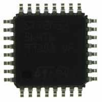
ST72F325K4T6 STMicroelectronics, ST72F325K4T6 Datasheet - Page 143

ST72F325K4T6
Manufacturer Part Number
ST72F325K4T6
Description
MCU 8BIT 16KB FLASH/ROM 32-LQFP
Manufacturer
STMicroelectronics
Series
ST7r
Datasheet
1.ST72F325K6T6.pdf
(197 pages)
Specifications of ST72F325K4T6
Core Processor
ST7
Core Size
8-Bit
Speed
8MHz
Connectivity
I²C, SCI, SPI
Peripherals
LVD, POR, PWM, WDT
Number Of I /o
24
Program Memory Size
16KB (16K x 8)
Program Memory Type
FLASH
Ram Size
512 x 8
Voltage - Supply (vcc/vdd)
3.8 V ~ 5.5 V
Data Converters
A/D 16x10b
Oscillator Type
Internal
Operating Temperature
-40°C ~ 85°C
Package / Case
32-LQFP
Processor Series
ST72F3x
Core
ST7
Data Bus Width
8 bit
Data Ram Size
512 B
Interface Type
I2C, SCI, SPI
Maximum Clock Frequency
8 MHz
Number Of Programmable I/os
48
Number Of Timers
2
Maximum Operating Temperature
+ 85 C
Mounting Style
SMD/SMT
Development Tools By Supplier
ST7232X-EVAL, ST7232X-SK/RAIS, ST72325-D/RAIS, ST7MDT20-DVP3, ST7MDT20J-EMU3, ST7MDT20M-EMU3, STX-RLINK
Minimum Operating Temperature
- 40 C
On-chip Adc
10 bit, 16 Channel
For Use With
497-5046 - KIT TOOL FOR ST7/UPSD/STR7 MCU
Lead Free Status / RoHS Status
Lead free / RoHS Compliant
Eeprom Size
-
Lead Free Status / Rohs Status
Details
Other names
497-5605
Available stocks
Company
Part Number
Manufacturer
Quantity
Price
Company:
Part Number:
ST72F325K4T6
Manufacturer:
ST
Quantity:
151
Company:
Part Number:
ST72F325K4T6
Manufacturer:
STMicroelectronics
Quantity:
10 000
Part Number:
ST72F325K4T6
Manufacturer:
ST
Quantity:
20 000
Company:
Part Number:
ST72F325K4T6TR
Manufacturer:
STMicroelectronics
Quantity:
10 000
12.2 ABSOLUTE MAXIMUM RATINGS
Stresses above those listed as “absolute maxi-
mum ratings” may cause permanent damage to
the device. This is a stress rating only and func-
tional operation of the device under these condi-
12.2.1 Voltage Characteristics
12.2.2 Current Characteristics
Notes:
1. Directly connecting the RESET and I/O pins to V
is generated or an unexpected change of the I/O configuration occurs (for example, due to a corrupted program counter).
To guarantee safe operation, this connection has to be done through a pull-up or pull-down resistor (typical: 4.7kΩ for
RESET, 10kΩ for I/Os). For the same reason, unused I/O pins must not be directly tied to V
2. I
respected, the injection current must be limited externally to the I
while a negative injection is induced by V
corresponding V
3. All power (V
4. Negative injection disturbs the analog performance of the device. See note in
For best reliability, it is recommended to avoid negative injection of more than 1.6mA.
5. When several inputs are submitted to a current injection, the maximum ΣI
and negative injected currents (instantaneous values). These results are based on characterisation with ΣI
mum current injection on four I/O port pins of the device.
6. True open drain I/O port pins do not accept positive injection.
|ΔV
INJ(PIN)
I
DDx
|V
I
INJ(PIN)
VDD
ΣI
V
V
V
V
V
SSA
Symbol
Symbol
ESD(HBM)
DD
INJ(PIN)
PP
IN
ESD(MM)
| and |ΔV
/ I
must never be exceeded. This is implicitly insured if V
I
1) & 2)
IO
- V
- V
- V
VSS
2) & 4)
DD
SS
SS
SSx
2)
IN
3)
) and ground (V
|
SSx
maximum must always be respected
|
Supply voltage
Programming Voltage
Input Voltage on true open drain pin
Input voltage on any other pin
Variations between different digital power pins
Variations between digital and analog ground pins
Electro-static discharge voltage (Human Body Model)
Electro-static discharge voltage (Machine Model)
Total current into V
(source) and V
Output current sunk by any standard I/O and control pin
Output current sunk by any high sink I/O pin
Output current source by any I/Os and control pin
Injected current on V
Injected current on RESET pin
Injected current on OSC1 and OSC2 pins
Injected current on PB0 (Flash devices only)
Injected current on any other pin
Total injected current (sum of all I/O and control pins)
SS
) lines must always be connected to the external supply.
SS
IN
<V
ground lines (sink)
DD
SS
PP
. For true open-drain pads, there is no positive injection current, and the
power lines
Ratings
Ratings
pin
DD
or V
5) & 6)
SS
could damage the device if an unintentional internal reset
tions is not implied. Exposure to maximum rating
conditions for extended periods may affect device
reliability.
INJ(PIN)
IN
32-pin devices
44/48/64-pin
devices
maximum is respected. If V
value. A positive injection is induced by V
INJ(PIN)
5)
“ADC Accuracy” on page
see
is the absolute sum of the positive
V
Maximum value
Maximum value
SS
section 12.7.3 on page 158
V
-0.3 to V
SS
-0.3 to 6.5
DD
± 25
150
- 25
± 5
± 5
± 5
+ 5
± 5
75
25
50
6.5
13
50
50
or V
IN
DD
SS
maximum cannot be
+0.3
.
ST72325xx
173.
INJ(PIN)
Unit
Unit
mA
mA
143/197
mV
IN
V
maxi-
>V
DD


