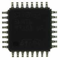
ST72F325K4T6 STMicroelectronics, ST72F325K4T6 Datasheet - Page 16

ST72F325K4T6
Manufacturer Part Number
ST72F325K4T6
Description
MCU 8BIT 16KB FLASH/ROM 32-LQFP
Manufacturer
STMicroelectronics
Series
ST7r
Datasheet
1.ST72F325K6T6.pdf
(197 pages)
Specifications of ST72F325K4T6
Core Processor
ST7
Core Size
8-Bit
Speed
8MHz
Connectivity
I²C, SCI, SPI
Peripherals
LVD, POR, PWM, WDT
Number Of I /o
24
Program Memory Size
16KB (16K x 8)
Program Memory Type
FLASH
Ram Size
512 x 8
Voltage - Supply (vcc/vdd)
3.8 V ~ 5.5 V
Data Converters
A/D 16x10b
Oscillator Type
Internal
Operating Temperature
-40°C ~ 85°C
Package / Case
32-LQFP
Processor Series
ST72F3x
Core
ST7
Data Bus Width
8 bit
Data Ram Size
512 B
Interface Type
I2C, SCI, SPI
Maximum Clock Frequency
8 MHz
Number Of Programmable I/os
48
Number Of Timers
2
Maximum Operating Temperature
+ 85 C
Mounting Style
SMD/SMT
Development Tools By Supplier
ST7232X-EVAL, ST7232X-SK/RAIS, ST72325-D/RAIS, ST7MDT20-DVP3, ST7MDT20J-EMU3, ST7MDT20M-EMU3, STX-RLINK
Minimum Operating Temperature
- 40 C
On-chip Adc
10 bit, 16 Channel
For Use With
497-5046 - KIT TOOL FOR ST7/UPSD/STR7 MCU
Lead Free Status / RoHS Status
Lead free / RoHS Compliant
Eeprom Size
-
Lead Free Status / Rohs Status
Details
Other names
497-5605
Available stocks
Company
Part Number
Manufacturer
Quantity
Price
Company:
Part Number:
ST72F325K4T6
Manufacturer:
ST
Quantity:
151
Company:
Part Number:
ST72F325K4T6
Manufacturer:
STMicroelectronics
Quantity:
10 000
Part Number:
ST72F325K4T6
Manufacturer:
ST
Quantity:
20 000
Company:
Part Number:
ST72F325K4T6TR
Manufacturer:
STMicroelectronics
Quantity:
10 000
ST72325xx
Notes for
1. In the interrupt input column, “eiX” defines the associated external interrupt vector. If the weak pull-up
column (wpu) is merged with the interrupt column (int), then the I/O configuration is pull-up interrupt input,
else the configuration is floating interrupt input.
2. In the open drain output column, “T” defines a true open drain I/O (P-Buffer and protection diode to V
are not implemented). See See “I/O PORTS” on page 50. and
ISTICS
3. OSC1 and OSC2 pins connect a crystal/ceramic resonator, or an external source to the on-chip oscil-
lator; see
more details.
4. On the chip, each I/O port may have up to 8 pads:
– In all devices except 48-pin ST72325C, pads that are not bonded to external pins are forced by hardware
– In 48-pin ST72325C devices, unbonded pads PA0, PA1, PB6, PB7, PD6, PD7, PE3, PE5, PE6, PE7,
5.
6.
pins to ground.
16/197
28 31 PB0/PWM3
29 32 PB3/PWM0
30
31
32
Pin n°
in input pull-up configuration after reset. The configuration of these pads must be kept at reset state to
avoid added current consumption.
PF3 and PF5) are in input floating configuration after reset. To avoid added current consumption, the
application must force these ports in input pull-up state by writing to the OR and DDR registers after re-
set. This initialization is not necessary in 48-pin ST72325S devices.
Pull-up always activated on PE2 see limitation
It is mandatory to connect all available V
1
2
3
for more details.
PB4 (HS)/ARTCLK
PD0/AIN0
PD1/AIN1
Table 2
Section 1 DESCRIPTION
Pin Name
and
Table
I/O C
I/O C
I/O C
I/O C
I/O C
3:
Level
T
T
T
T
T
HS
and
Section 12.5 CLOCK AND TIMING CHARACTERISTICS
X
X
X
X
X
DD
X
X
Input
ei2
ei3
and V
ei2
Port
Section
REF
X
X
Output
pins to the supply voltage and all V
X
X
X
X
X
15.1.8.
Section 12.8 I/O PORT PIN CHARACTER-
X
X
X
X
X
function
Port B0
Port B3
Port B4
Port D0
Port D1
reset)
(after
Main
PWM Output 3
Caution: Negative current injec-
tion not allowed on this pin
PWM Output 0
PWM-ART External Clock
ADC Analog Input 0
ADC Analog Input 1
Alternate function
SS
and V
SSA
for
DD


