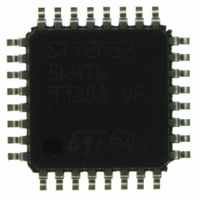
ST72F325K4T6 STMicroelectronics, ST72F325K4T6 Datasheet - Page 35

ST72F325K4T6
Manufacturer Part Number
ST72F325K4T6
Description
MCU 8BIT 16KB FLASH/ROM 32-LQFP
Manufacturer
STMicroelectronics
Series
ST7r
Datasheet
1.ST72F325K6T6.pdf
(197 pages)
Specifications of ST72F325K4T6
Core Processor
ST7
Core Size
8-Bit
Speed
8MHz
Connectivity
I²C, SCI, SPI
Peripherals
LVD, POR, PWM, WDT
Number Of I /o
24
Program Memory Size
16KB (16K x 8)
Program Memory Type
FLASH
Ram Size
512 x 8
Voltage - Supply (vcc/vdd)
3.8 V ~ 5.5 V
Data Converters
A/D 16x10b
Oscillator Type
Internal
Operating Temperature
-40°C ~ 85°C
Package / Case
32-LQFP
Processor Series
ST72F3x
Core
ST7
Data Bus Width
8 bit
Data Ram Size
512 B
Interface Type
I2C, SCI, SPI
Maximum Clock Frequency
8 MHz
Number Of Programmable I/os
48
Number Of Timers
2
Maximum Operating Temperature
+ 85 C
Mounting Style
SMD/SMT
Development Tools By Supplier
ST7232X-EVAL, ST7232X-SK/RAIS, ST72325-D/RAIS, ST7MDT20-DVP3, ST7MDT20J-EMU3, ST7MDT20M-EMU3, STX-RLINK
Minimum Operating Temperature
- 40 C
On-chip Adc
10 bit, 16 Channel
For Use With
497-5046 - KIT TOOL FOR ST7/UPSD/STR7 MCU
Lead Free Status / RoHS Status
Lead free / RoHS Compliant
Eeprom Size
-
Lead Free Status / Rohs Status
Details
Other names
497-5605
Available stocks
Company
Part Number
Manufacturer
Quantity
Price
Company:
Part Number:
ST72F325K4T6
Manufacturer:
ST
Quantity:
151
Company:
Part Number:
ST72F325K4T6
Manufacturer:
STMicroelectronics
Quantity:
10 000
Part Number:
ST72F325K4T6
Manufacturer:
ST
Quantity:
20 000
Company:
Part Number:
ST72F325K4T6TR
Manufacturer:
STMicroelectronics
Quantity:
10 000
SYSTEM INTEGRITY MANAGEMENT (Cont’d)
6.4.5 Register Description
SYSTEM INTEGRITY (SI) CONTROL/STATUS REGISTER (SICSR)
Read/Write
Reset Value: 000x 000x (00h)
Bit 7 = AVDS Voltage Detection selection
This bit is set and cleared by software. Voltage De-
tection is available only if the LVD is enabled by
option byte.
0: Voltage detection on V
1: Voltage detection on EVD pin
Bit 6 = AVDIE Voltage Detector interrupt enable
This bit is set and cleared by software. It enables
an interrupt to be generated when the AVDF flag
changes (toggles). The pending interrupt informa-
tion is automatically cleared when software enters
the AVD interrupt routine.
0: AVD interrupt disabled
1: AVD interrupt enabled
Bit 5 = AVDF Voltage Detector flag
This read-only bit is set and cleared by hardware.
If the AVDIE bit is set, an interrupt request is gen-
erated when the AVDF bit changes value. Refer to
Figure 18
tails.
0: V
1: V
Bit 4 = LVDRF LVD reset flag
This bit indicates that the last Reset was generat-
ed by the LVD block. It is set by hardware (LVD re-
set) and cleared by software (writing zero). See
WDGRF flag description for more details. When
the LVD is disabled by OPTION BYTE, the LVDRF
bit value is undefined.
Bit 3 = Reserved, must be kept cleared.
Bit 2 = CSSIE Clock security syst
This bit enables the interrupt when a disturbance
AVD
S
7
DD
DD
or V
or V
AVD
IE
and to
EVD
EVD
AVD
F
over V
under V
Section 6.4.2.1
LVD
RF
IT+(AVD)
IT-(AVD)
DD
0
supply
threshold
threshold
CSS
for additional de-
.
IE
interrupt enable
CSS
D
WDG
RF
0
is detected by the Clock Security System (CSSD
bit set). It is set and cleared by software.
0: Clock security system interrupt disabled
1: Clock security system interrupt enabled
When the CSS is disabled by OPTION BYTE, the
CSSIE bit has no effect.
Bit 1 = CSSD Clock security system detection
This bit indicates that the safe oscillator of the
Clock Security System block has been selected by
hardware due to a disturbance on the main clock
signal (f
reading the SICSR register when the original oscil-
lator recovers.
0: Safe oscillator is not active
1: Safe oscillator has been activated
When the CSS is disabled by OPTION BYTE, the
CSSD bit value is forced to 0.
Bit 0 = WDGRF Watchdog reset flag
This bit indicates that the last Reset was generat-
ed by the Watchdog peripheral. It is set by hard-
ware (watchdog reset) and cleared by software
(writing zero) or an LVD Reset (to ensure a stable
cleared state of the WDGRF flag when CPU
starts).
Combined with the LVDRF flag information, the
flag description is given by the following table.
Application notes
The LVDRF flag is not cleared when another RE-
SET type occurs (external or watchdog), the
LVDRF flag remains set to keep trace of the origi-
nal failure.
In this case, a watchdog reset can be detected by
software while an external reset can not.
CAUTION: When the LVD is not activated with the
associated option byte, the WDGRF flag can not
be used in the application.
External RESET pin
OSC
RESET Sources
Watchdog
). It is set by hardware and cleared by
LVD
LVDRF
0
1
0
ST72325xx
WDGRF
35/197
X
0
1


