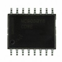
MC908QY8CDWE Freescale Semiconductor, MC908QY8CDWE Datasheet - Page 113

MC908QY8CDWE
Manufacturer Part Number
MC908QY8CDWE
Description
IC MCU 8BIT 8K FLASH 16-SOIC
Manufacturer
Freescale Semiconductor
Series
HC08r
Datasheet
1.MC908QB8CDWE.pdf
(236 pages)
Specifications of MC908QY8CDWE
Core Processor
HC08
Core Size
8-Bit
Speed
8MHz
Peripherals
LVD, POR, PWM
Number Of I /o
13
Program Memory Size
8KB (8K x 8)
Program Memory Type
FLASH
Ram Size
256 x 8
Voltage - Supply (vcc/vdd)
2.7 V ~ 5.5 V
Data Converters
A/D 4x10b
Oscillator Type
External
Operating Temperature
-40°C ~ 85°C
Package / Case
16-SOIC (0.300", 7.5mm Width)
Processor Series
HC08QY
Core
HC08
Data Bus Width
8 bit
Data Ram Size
256 B
Maximum Clock Frequency
8 MHz
Number Of Programmable I/os
13
Number Of Timers
2
Operating Supply Voltage
3 V to 5 V
Maximum Operating Temperature
+ 85 C
Mounting Style
SMD/SMT
Development Tools By Supplier
FSICEBASE, M68CBL05AE, DEMO908QB8, DEMO908QC16
Minimum Operating Temperature
- 40 C
On-chip Adc
4-ch x 10-bit
Lead Free Status / RoHS Status
Lead free / RoHS Compliant
Eeprom Size
-
Connectivity
-
Lead Free Status / Rohs Status
Lead free / RoHS Compliant
Available stocks
Company
Part Number
Manufacturer
Quantity
Price
Company:
Part Number:
MC908QY8CDWE
Manufacturer:
Winbond
Quantity:
16 700
Part Number:
MC908QY8CDWE
Manufacturer:
FREESCALE
Quantity:
20 000
- Current page: 113 of 236
- Download datasheet (3Mb)
13.3.2.1 Character Length
The transmitter can accommodate either 8-bit or 9-bit data. The state of the M bit in ESCI control
register 1 (SCC1) determines character length. When transmitting 9-bit data, bit T8 in ESCI control
register 3 (SCC3) is the ninth bit (bit 8).
13.3.2.2 Character Transmission
During an ESCI transmission, the transmit shift register shifts a character out to the TxD pin. The ESCI
data register (SCDR) is the write-only buffer between the internal data bus and the transmit shift register.
To initiate an ESCI transmission:
At the start of a transmission, transmitter control logic automatically loads the transmit shift register with
a preamble of 1s. After the preamble shifts out, control logic transfers the SCDR data into the transmit
shift register. A 0 start bit automatically goes into the least significant bit (LSB) position of the transmit shift
register. A 1 stop bit goes into the most significant bit (MSB) position.
The ESCI transmitter empty bit, SCTE, in SCS1 becomes set when the SCDR transfers a byte to the
transmit shift register. The SCTE bit indicates that the SCDR can accept new data from the internal data
bus. If the ESCI transmit interrupt enable bit, SCTIE, in SCC2 is also set, the SCTE bit generates a
transmitter interrupt request.
When the transmit shift register is not transmitting a character, the TxD pin goes to the idle condition, high.
If at any time software clears the ENSCI bit in ESCI control register 1 (SCC1), the transmitter and receiver
relinquish control of the port pins.
13.3.2.3 Break Characters
Writing a 1 to the send break bit, SBK, in SCC2 loads the transmit shift register with a break character.
For TXINV = 0 (output not inverted), a transmitted break character contains all 0s and has no start, stop,
or parity bit. Break character length depends on the M bit in SCC1 and the LINR bits in SCBR. As long as
SBK is set, transmitter logic continuously loads break characters into the transmit shift register. After
software clears the SBK bit, the shift register finishes transmitting the last break character and then
transmits at least one 1. The automatic 1 at the end of a break character guarantees the recognition of
the start bit of the next character.
When LINR is cleared in SCBR, the ESCI recognizes a break character when a start bit is followed by
eight or nine 0 data bits and a 0 where the stop bit should be, resulting in a total of 10 or 11 consecutive 0
data bits. When LINR is set in SCBR, the ESCI recognizes a break character when a start bit is followed
by 9 or 10 0 data bits and a 0 where the stop bit should be, resulting in a total of 11 or 12 consecutive 0
data bits.
Freescale Semiconductor
1. Enable the ESCI by writing a 1 to the enable ESCI bit (ENSCI) in ESCI control register 1 (SCC1).
2. Enable the transmitter by writing a 1 to the transmitter enable bit (TE) in ESCI control register 2
3. Clear the ESCI transmitter empty bit (SCTE) by first reading ESCI status register 1 (SCS1) and
4. Repeat step 3 for each subsequent transmission.
(SCC2).
then writing to the SCDR. For 9-bit data, also write the T8 bit in SCC3.
MC68HC908QB8 Data Sheet, Rev. 3
Functional Description
113
Related parts for MC908QY8CDWE
Image
Part Number
Description
Manufacturer
Datasheet
Request
R
Part Number:
Description:
Manufacturer:
Freescale Semiconductor, Inc
Datasheet:
Part Number:
Description:
Manufacturer:
Freescale Semiconductor, Inc
Datasheet:
Part Number:
Description:
Manufacturer:
Freescale Semiconductor, Inc
Datasheet:
Part Number:
Description:
Manufacturer:
Freescale Semiconductor, Inc
Datasheet:
Part Number:
Description:
Manufacturer:
Freescale Semiconductor, Inc
Datasheet:
Part Number:
Description:
Manufacturer:
Freescale Semiconductor, Inc
Datasheet:
Part Number:
Description:
Manufacturer:
Freescale Semiconductor, Inc
Datasheet:
Part Number:
Description:
Manufacturer:
Freescale Semiconductor, Inc
Datasheet:
Part Number:
Description:
Manufacturer:
Freescale Semiconductor, Inc
Datasheet:
Part Number:
Description:
Manufacturer:
Freescale Semiconductor, Inc
Datasheet:
Part Number:
Description:
Manufacturer:
Freescale Semiconductor, Inc
Datasheet:
Part Number:
Description:
Manufacturer:
Freescale Semiconductor, Inc
Datasheet:
Part Number:
Description:
Manufacturer:
Freescale Semiconductor, Inc
Datasheet:
Part Number:
Description:
Manufacturer:
Freescale Semiconductor, Inc
Datasheet:
Part Number:
Description:
Manufacturer:
Freescale Semiconductor, Inc
Datasheet:


