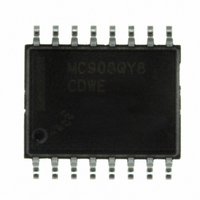
MC908QY8CDWE Freescale Semiconductor, MC908QY8CDWE Datasheet - Page 125

MC908QY8CDWE
Manufacturer Part Number
MC908QY8CDWE
Description
IC MCU 8BIT 8K FLASH 16-SOIC
Manufacturer
Freescale Semiconductor
Series
HC08r
Datasheet
1.MC908QB8CDWE.pdf
(236 pages)
Specifications of MC908QY8CDWE
Core Processor
HC08
Core Size
8-Bit
Speed
8MHz
Peripherals
LVD, POR, PWM
Number Of I /o
13
Program Memory Size
8KB (8K x 8)
Program Memory Type
FLASH
Ram Size
256 x 8
Voltage - Supply (vcc/vdd)
2.7 V ~ 5.5 V
Data Converters
A/D 4x10b
Oscillator Type
External
Operating Temperature
-40°C ~ 85°C
Package / Case
16-SOIC (0.300", 7.5mm Width)
Processor Series
HC08QY
Core
HC08
Data Bus Width
8 bit
Data Ram Size
256 B
Maximum Clock Frequency
8 MHz
Number Of Programmable I/os
13
Number Of Timers
2
Operating Supply Voltage
3 V to 5 V
Maximum Operating Temperature
+ 85 C
Mounting Style
SMD/SMT
Development Tools By Supplier
FSICEBASE, M68CBL05AE, DEMO908QB8, DEMO908QC16
Minimum Operating Temperature
- 40 C
On-chip Adc
4-ch x 10-bit
Lead Free Status / RoHS Status
Lead free / RoHS Compliant
Eeprom Size
-
Connectivity
-
Lead Free Status / Rohs Status
Lead free / RoHS Compliant
Available stocks
Company
Part Number
Manufacturer
Quantity
Price
Company:
Part Number:
MC908QY8CDWE
Manufacturer:
Winbond
Quantity:
16 700
Part Number:
MC908QY8CDWE
Manufacturer:
FREESCALE
Quantity:
20 000
- Current page: 125 of 236
- Download datasheet (3Mb)
RWU — Receiver Wakeup Bit
SBK — Send Break Bit
13.8.3 ESCI Control Register 3
ESCI control register 3 (SCC3):
R8 — Received Bit 8
T8 — Transmitted Bit 8
Freescale Semiconductor
This read/write bit puts the receiver in a standby state during which receiver interrupts are disabled.
The WAKE bit in SCC1 determines whether an idle input or an address mark brings the receiver out
of the standby state and clears the RWU bit.
Setting and then clearing this read/write bit transmits a break character followed by a 1. The 1 after the
break character guarantees recognition of a valid start bit. If SBK remains set, the transmitter
continuously transmits break characters with no 1s between them.
•
•
When the ESCI is receiving 9-bit characters, R8 is the read-only ninth bit (bit 8) of the received
character. R8 is received at the same time that the SCDR receives the other 8 bits.
When the ESCI is receiving 8-bit characters, R8 is a copy of the eighth bit (bit 7).
When the ESCI is transmitting 9-bit characters, T8 is the read/write ninth bit (bit 8) of the transmitted
character. T8 is loaded into the transmit shift register at the same time that the SCDR is loaded into
the transmit shift register.
1 = Standby state
0 = Normal operation
1 = Transmit break characters
0 = No break characters being transmitted
Stores the ninth ESCI data bit received and the ninth ESCI data bit to be transmitted.
Enables these interrupts:
–
–
–
–
Receiver overrun
Noise error
Framing error
Parity error
Reset:
Read:
Write:
Writing to the RE bit is not allowed when the enable ESCI bit (ENSCI) is
clear. ENSCI is in ESCI control register 1.
Do not toggle the SBK bit immediately after setting the SCTE bit. Toggling
SBK before the preamble begins causes the ESCI to send a break
character instead of a preamble.
Bit 7
R8
U
Figure 13-11. ESCI Control Register 3 (SCC3)
= Unimplemented
T8
6
0
MC68HC908QB8 Data Sheet, Rev. 3
R
5
0
NOTE
NOTE
R
R
4
0
= Reserved
ORIE
3
0
NEIE
U = Unaffected
2
0
FEIE
1
0
PEIE
Bit 0
0
Registers
125
Related parts for MC908QY8CDWE
Image
Part Number
Description
Manufacturer
Datasheet
Request
R
Part Number:
Description:
Manufacturer:
Freescale Semiconductor, Inc
Datasheet:
Part Number:
Description:
Manufacturer:
Freescale Semiconductor, Inc
Datasheet:
Part Number:
Description:
Manufacturer:
Freescale Semiconductor, Inc
Datasheet:
Part Number:
Description:
Manufacturer:
Freescale Semiconductor, Inc
Datasheet:
Part Number:
Description:
Manufacturer:
Freescale Semiconductor, Inc
Datasheet:
Part Number:
Description:
Manufacturer:
Freescale Semiconductor, Inc
Datasheet:
Part Number:
Description:
Manufacturer:
Freescale Semiconductor, Inc
Datasheet:
Part Number:
Description:
Manufacturer:
Freescale Semiconductor, Inc
Datasheet:
Part Number:
Description:
Manufacturer:
Freescale Semiconductor, Inc
Datasheet:
Part Number:
Description:
Manufacturer:
Freescale Semiconductor, Inc
Datasheet:
Part Number:
Description:
Manufacturer:
Freescale Semiconductor, Inc
Datasheet:
Part Number:
Description:
Manufacturer:
Freescale Semiconductor, Inc
Datasheet:
Part Number:
Description:
Manufacturer:
Freescale Semiconductor, Inc
Datasheet:
Part Number:
Description:
Manufacturer:
Freescale Semiconductor, Inc
Datasheet:
Part Number:
Description:
Manufacturer:
Freescale Semiconductor, Inc
Datasheet:


