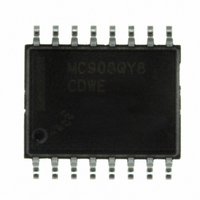
MC908QY8CDWE Freescale Semiconductor, MC908QY8CDWE Datasheet - Page 96

MC908QY8CDWE
Manufacturer Part Number
MC908QY8CDWE
Description
IC MCU 8BIT 8K FLASH 16-SOIC
Manufacturer
Freescale Semiconductor
Series
HC08r
Datasheet
1.MC908QB8CDWE.pdf
(236 pages)
Specifications of MC908QY8CDWE
Core Processor
HC08
Core Size
8-Bit
Speed
8MHz
Peripherals
LVD, POR, PWM
Number Of I /o
13
Program Memory Size
8KB (8K x 8)
Program Memory Type
FLASH
Ram Size
256 x 8
Voltage - Supply (vcc/vdd)
2.7 V ~ 5.5 V
Data Converters
A/D 4x10b
Oscillator Type
External
Operating Temperature
-40°C ~ 85°C
Package / Case
16-SOIC (0.300", 7.5mm Width)
Processor Series
HC08QY
Core
HC08
Data Bus Width
8 bit
Data Ram Size
256 B
Maximum Clock Frequency
8 MHz
Number Of Programmable I/os
13
Number Of Timers
2
Operating Supply Voltage
3 V to 5 V
Maximum Operating Temperature
+ 85 C
Mounting Style
SMD/SMT
Development Tools By Supplier
FSICEBASE, M68CBL05AE, DEMO908QB8, DEMO908QC16
Minimum Operating Temperature
- 40 C
On-chip Adc
4-ch x 10-bit
Lead Free Status / RoHS Status
Lead free / RoHS Compliant
Eeprom Size
-
Connectivity
-
Lead Free Status / Rohs Status
Lead free / RoHS Compliant
Available stocks
Company
Part Number
Manufacturer
Quantity
Price
Company:
Part Number:
MC908QY8CDWE
Manufacturer:
Winbond
Quantity:
16 700
Part Number:
MC908QY8CDWE
Manufacturer:
FREESCALE
Quantity:
20 000
Oscillator Module (OSC)
Figure 11-3
OSC2EN.
11.3.2.1 Internal Oscillator Trimming
OSCTRIM allows a clock period adjustment of +127 and –128 steps. Increasing the OSCTRIM value
increases the clock period, which decreases the clock frequency. Trimming allows the internal clock
frequency to be fine tuned to the target frequency.
All devices are factory programmed with a trim value that is stored in FLASH memory at location $FFC0.
The trim value is not automatically loaded into the OSCTRIM register. User software must copy the trim
value from $FFC0 into OSCTRIM if needed. The factory trim value provides the accuracy required for
communication using forced monitor mode. Some production programmers erase the factory trim value,
so confirm with your programmer vendor that the trim value at $FFC0 is preserved, or is re-trimmed.
Trimming the device in the user application board will provide the most accurate trim value.
11.3.2.2 Internal to External Clock Switching
When external clock source (external OSC, RC, or XTAL) is desired, the user must perform the following
steps:
After ECGON set is detected, the OSC module checks for oscillator activity by waiting two external clock
rising edges. The OSC module then switches to the external clock. Logic provides a coherent transition.
The OSC module first sets ECGST and then stops the internal oscillator.
11.3.2.3 External to Internal Clock Switching
After following the procedures to switch to an external clock source, it is possible to go back to the internal
source. By clearing the OSCOPT[1:0] bits and clearing the ECGON bit, the external circuit will be
disengaged. The bus clock will be derived from the selected internal clock source based on the ICFS[1:0]
bits.
11.3.3 External Oscillator
The external oscillator option is designed for use when a clock signal is available in the application to
provide a clock source to the MCU. The OSC1 pin is enabled as an input by the oscillator module. The
clock signal is used directly to create BUSCLKX4 and also divided by two to create BUSCLKX2.
In this configuration, the OSC2 pin cannot output BUSCLKX4. The OSC2EN bit will be forced clear to
enable alternative functions on the pin.
96
1. For external crystal circuits only, configure OSCOPT[1:0] to external crystal. To help precharge an
2. Configure OSCOPT[1:0] and ECFS[1:0] according to
3. Create a software delay to provide the stabilization time required for the selected clock source
4. After the stabilization delay has elapsed, set ECGON.
external crystal oscillator, momentarily configure OSC2 as an output and drive it high for several
cycles. This can help the crystal circuit start more robustly.
The oscillator module control logic will then enable OSC1 as an external clock input and, if the
external crystal option is selected, OSC2 will also be enabled as the clock output. If RC oscillator
option is selected, enabling the OSC2 output may change the bus frequency.
(crystal, resonator, RC). A good rule of thumb for crystal oscillators is to wait 4096 cycles of the
crystal frequency; i.e., for a 4-MHz crystal, wait approximately 1 ms.
shows how BUSCLKX4 is derived from INTCLK and OSC2 can output BUSCLKX4 by setting
MC68HC908QB8 Data Sheet, Rev. 3
11.8.1 Oscillator Status and Control
Freescale Semiconductor
Register.


