DF70845AD80FPV Renesas Electronics America, DF70845AD80FPV Datasheet - Page 1316
DF70845AD80FPV
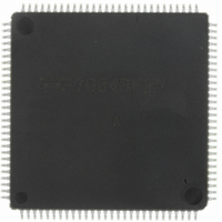
Manufacturer Part Number
DF70845AD80FPV
Description
IC SUPERH MCU FLASH 112LQFP
Manufacturer
Renesas Electronics America
Series
SuperH® SH7080r
Datasheet
1.DF70844AD80FPV.pdf
(1644 pages)
Specifications of DF70845AD80FPV
Core Size
32-Bit
Program Memory Size
512KB (512K x 8)
Core Processor
SH-2
Speed
80MHz
Connectivity
EBI/EMI, FIFO, I²C, SCI, SSU
Peripherals
DMA, POR, PWM, WDT
Number Of I /o
76
Program Memory Type
FLASH
Ram Size
32K x 8
Voltage - Supply (vcc/vdd)
3 V ~ 5.5 V
Data Converters
A/D 8x10b
Oscillator Type
Internal
Operating Temperature
-40°C ~ 85°C
Package / Case
112-LQFP
No. Of I/o's
76
Ram Memory Size
32KB
Cpu Speed
80MHz
Digital Ic Case Style
LQFP
Supply Voltage Range
3V To 3.6V, 4.5V To 5.5V
Embedded Interface Type
I2C, SCI
Rohs Compliant
Yes
Lead Free Status / RoHS Status
Lead free / RoHS Compliant
For Use With
R0K570865S001BE - KIT STARTER FOR SH7086R0K570865S000BE - KIT STARTER FOR SH7086HS0005KCU11H - EMULATOR E10A-USB H8S(X),SH2(A)
Eeprom Size
-
Lead Free Status / RoHS Status
Lead free / RoHS Compliant, Lead free / RoHS Compliant
Available stocks
Company
Part Number
Manufacturer
Quantity
Price
Company:

Part Number:
DF70845AD80FPV
Manufacturer:
TAIYO
Quantity:
40 000
Company:
Part Number:
DF70845AD80FPV
Manufacturer:
Renesas Electronics America
Quantity:
10 000


Section 23 Flash Memory
(2) Programming Procedure in User Program Mode
Rev. 3.00 May 17, 2007 Page 1258 of 1582
REJ09B0181-0300
The procedures for download, initialization, and programming are shown in figure 23.11.
The details of the programming procedure are described below. The procedure program must
be executed in an area other than the flash memory to be programmed. Especially the part
where the SCO bit in FCCS is set to 1 for downloading must be executed in the on-chip RAM.
Specify 1/4 (initial value) as the frequency division ratios of an internal clock (Iφ), a bus clock
(Bφ), and a peripheral clock (Pφ) through the frequency control register (FRQCR).
After the programming/erasing program has been downloaded and the SCO bit is cleared to 0,
the setting of the frequency control register (FRQCR) can be changed to the desired value.
The area that can be executed in the steps of the user procedure program (on-chip RAM, user
MAT, and external space) is shown in section 23.9.2, Areas for Storage of the Procedural
Program and Data for Programming.
set download destination
JSR FTDAR setting+32
Select on-chip program
to be downloaded and
Set the FPEFEQ and
After clearing VBR,
FUBRA parameters
procedure program
execute download
set SCO to 1 and
Start programming
Set FKEY to H'A5
Clear FKEY to 0
Initialization
DPFR=0?
FPFR=0?
by FTDAR
1
Yes
Yes
Initialization error processing
Download error processing
No
No
Figure 23.11 Programming Procedure
(2.1)
(2.2)
(2.3)
(2.4)
(2.5)
(2.6)
(2.7)
(2.8)
No
R5 (FMPAR and FMPDR)
Set parameter to R4 and
JSR FTDAR setting+16
procedure program
End programming
Set FKEY to H'5A
Clear FKEY to 0
programming is
Programming
Required data
completed?
FPFR=0?
1
Yes
Yes
Clear FKEY and
error processing
No
programming
(2.9)
(2.10)
(2.11)
(2.12)
(2.13)
(2.14)
Related parts for DF70845AD80FPV
Image
Part Number
Description
Manufacturer
Datasheet
Request
R

Part Number:
Description:
KIT STARTER FOR M16C/29
Manufacturer:
Renesas Electronics America
Datasheet:

Part Number:
Description:
KIT STARTER FOR R8C/2D
Manufacturer:
Renesas Electronics America
Datasheet:

Part Number:
Description:
R0K33062P STARTER KIT
Manufacturer:
Renesas Electronics America
Datasheet:

Part Number:
Description:
KIT STARTER FOR R8C/23 E8A
Manufacturer:
Renesas Electronics America
Datasheet:

Part Number:
Description:
KIT STARTER FOR R8C/25
Manufacturer:
Renesas Electronics America
Datasheet:

Part Number:
Description:
KIT STARTER H8S2456 SHARPE DSPLY
Manufacturer:
Renesas Electronics America
Datasheet:

Part Number:
Description:
KIT STARTER FOR R8C38C
Manufacturer:
Renesas Electronics America
Datasheet:

Part Number:
Description:
KIT STARTER FOR R8C35C
Manufacturer:
Renesas Electronics America
Datasheet:

Part Number:
Description:
KIT STARTER FOR R8CL3AC+LCD APPS
Manufacturer:
Renesas Electronics America
Datasheet:
Part Number:
Description:
KIT STARTER FOR RX610
Manufacturer:
Renesas Electronics America
Datasheet:

Part Number:
Description:
KIT STARTER FOR R32C/118
Manufacturer:
Renesas Electronics America
Datasheet:

Part Number:
Description:
KIT DEV RSK-R8C/26-29
Manufacturer:
Renesas Electronics America
Datasheet:

Part Number:
Description:
KIT STARTER FOR SH7124
Manufacturer:
Renesas Electronics America
Datasheet:

Part Number:
Description:
KIT STARTER FOR H8SX/1622
Manufacturer:
Renesas Electronics America
Datasheet:

Part Number:
Description:
KIT DEV FOR SH7203
Manufacturer:
Renesas Electronics America
Datasheet: