DF61543J40FPV Renesas Electronics America, DF61543J40FPV Datasheet - Page 14
DF61543J40FPV
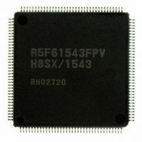
Manufacturer Part Number
DF61543J40FPV
Description
IC H8SX/1543 MCU FLASH 144-LQFP
Manufacturer
Renesas Electronics America
Series
H8® H8SX/1500r
Datasheet
1.DF61543J40FPV.pdf
(968 pages)
Specifications of DF61543J40FPV
Core Processor
H8SX
Core Size
32-Bit
Speed
40MHz
Connectivity
CAN, I²C, SCI, SSU
Peripherals
DMA, Motor Control PWM, PWM, WDT
Number Of I /o
95
Program Memory Size
384KB (384K x 8)
Program Memory Type
FLASH
Ram Size
16K x 8
Voltage - Supply (vcc/vdd)
4.5 V ~ 5.5 V
Data Converters
A/D 16x10b; D/A 2x8b
Operating Temperature
-20°C ~ 75°C
Package / Case
144-LQFP
For Use With
R0K561582S000BE - KIT DEV RSK H8SX/1582F
Lead Free Status / RoHS Status
Lead free / RoHS Compliant
Eeprom Size
-
Oscillator Type
-
Available stocks
Company
Part Number
Manufacturer
Quantity
Price
Company:

Part Number:
DF61543J40FPV
Manufacturer:
Renesas Electronics America
Quantity:
135
Company:
Part Number:
DF61543J40FPV
Manufacturer:
Renesas Electronics America
Quantity:
10 000


Section 6
6.1
6.2
6.3
6.4
6.5
6.6
6.7
6.8
6.9
6.10 Bus Arbitration .................................................................................................................. 184
Rev. 3.00 Sep. 24, 2009 Page xii of xlvi
REJ09B0381-0300
5.8.5
5.8.6
Features.............................................................................................................................. 131
Register Descriptions......................................................................................................... 133
6.2.1
6.2.2
6.2.3
6.2.4
6.2.5
6.2.6
6.2.7
6.2.8
Bus Configuration.............................................................................................................. 148
Multi-Clock Function and Number of Access Cycles ....................................................... 149
External Bus....................................................................................................................... 152
6.5.1
6.5.2
6.5.3
6.5.4
6.5.5
Basic Bus Interface ............................................................................................................ 162
6.6.1
6.6.2
6.6.3
6.6.4
6.6.5
6.6.6
Idle Cycle........................................................................................................................... 172
6.7.1
6.7.2
Internal Bus........................................................................................................................ 180
6.8.1
Write Data Buffer Function ............................................................................................... 182
6.9.1
6.9.2
6.10.1 Operation .............................................................................................................. 184
6.10.2 Bus Handover Timing........................................................................................... 184
Interrupts during Execution of MOVMD and MOVSD Instructions.................... 129
Interrupt Flags of Peripheral Modules .................................................................. 130
Bus Controller (BSC) ...................................................................... 131
Bus Width Control Register (ABWCR) ............................................................... 134
Access State Control Register (ASTCR) .............................................................. 135
Wait Control Registers A and B (WTCRA, WTCRB) ......................................... 136
Read Strobe Timing Control Register (RDNCR) ................................................. 141
Idle Control Register (IDLCR) ............................................................................. 142
Bus Control Register 1 (BCR1) ............................................................................ 144
Bus Control Register 2 (BCR2) ............................................................................ 146
Endian Control Register (ENDIANCR) ............................................................... 147
Input/Output Pins.................................................................................................. 152
Area Division........................................................................................................ 154
External Bus Interface .......................................................................................... 155
Area and External Bus Interface ........................................................................... 157
Endian and Data Alignment.................................................................................. 158
Data Bus ............................................................................................................... 162
I/O Pins Used for Basic Bus Interface .................................................................. 162
Basic Timing......................................................................................................... 163
Wait Control ......................................................................................................... 169
Read Strobe (RD) Timing..................................................................................... 170
DACK Signal Output Timing ............................................................................... 171
Operation .............................................................................................................. 172
Pin States in Idle Cycle......................................................................................... 180
Access to Internal Address Space ......................................................................... 180
Write Data Buffer Function for External Data Bus .............................................. 182
Write Data Buffer Function for Peripheral Modules ............................................ 183
Related parts for DF61543J40FPV
Image
Part Number
Description
Manufacturer
Datasheet
Request
R

Part Number:
Description:
KIT STARTER FOR M16C/29
Manufacturer:
Renesas Electronics America
Datasheet:

Part Number:
Description:
KIT STARTER FOR R8C/2D
Manufacturer:
Renesas Electronics America
Datasheet:

Part Number:
Description:
R0K33062P STARTER KIT
Manufacturer:
Renesas Electronics America
Datasheet:

Part Number:
Description:
KIT STARTER FOR R8C/23 E8A
Manufacturer:
Renesas Electronics America
Datasheet:

Part Number:
Description:
KIT STARTER FOR R8C/25
Manufacturer:
Renesas Electronics America
Datasheet:

Part Number:
Description:
KIT STARTER H8S2456 SHARPE DSPLY
Manufacturer:
Renesas Electronics America
Datasheet:

Part Number:
Description:
KIT STARTER FOR R8C38C
Manufacturer:
Renesas Electronics America
Datasheet:

Part Number:
Description:
KIT STARTER FOR R8C35C
Manufacturer:
Renesas Electronics America
Datasheet:

Part Number:
Description:
KIT STARTER FOR R8CL3AC+LCD APPS
Manufacturer:
Renesas Electronics America
Datasheet:
Part Number:
Description:
KIT STARTER FOR RX610
Manufacturer:
Renesas Electronics America
Datasheet:

Part Number:
Description:
KIT STARTER FOR R32C/118
Manufacturer:
Renesas Electronics America
Datasheet:

Part Number:
Description:
KIT DEV RSK-R8C/26-29
Manufacturer:
Renesas Electronics America
Datasheet:

Part Number:
Description:
KIT STARTER FOR SH7124
Manufacturer:
Renesas Electronics America
Datasheet:

Part Number:
Description:
KIT STARTER FOR H8SX/1622
Manufacturer:
Renesas Electronics America
Datasheet:

Part Number:
Description:
KIT DEV FOR SH7203
Manufacturer:
Renesas Electronics America
Datasheet: