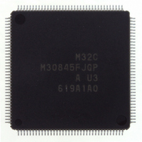
M30845FJGP#U3 Renesas Electronics America, M30845FJGP#U3 Datasheet - Page 333

M30845FJGP#U3
Manufacturer Part Number
M30845FJGP#U3
Description
IC M32C MCU FLASH 512K 144LQFP
Manufacturer
Renesas Electronics America
Series
M16C™ M32C/80r
Specifications of M30845FJGP#U3
Core Processor
M32C/80
Core Size
16/32-Bit
Speed
32MHz
Connectivity
CAN, I²C, IEBus, SIO, UART/USART
Peripherals
DMA, PWM, WDT
Number Of I /o
121
Program Memory Size
512KB (512K x 8)
Program Memory Type
FLASH
Ram Size
24K x 8
Voltage - Supply (vcc/vdd)
3 V ~ 5.5 V
Data Converters
A/D 34x10b, D/A 2x8b
Oscillator Type
Internal
Operating Temperature
-40°C ~ 85°C
Package / Case
144-LQFP
Lead Free Status / RoHS Status
Lead free / RoHS Compliant
Eeprom Size
-
Available stocks
Company
Part Number
Manufacturer
Quantity
Price
- Current page: 333 of 531
- Download datasheet (4Mb)
R
R
M
e
E
3
. v
J
2
NOTES:
NOTES:
Table 22.12 Clock Synchronous Serial I/O Mode Specifications (Communication Units 0 and 1)
Table 22.13 Clock Settings (Communication Unit 0)
9 0
C
22.4.1 Clock Synchronous Serial I/O Mode (Communication Units 0 and 1)
Transfer Data Format
Transfer Clock
Transmit Start Condition
Receive Start Condition
Interrupt Request
Error Detection
Selectable Function
. 1
Input from ISCLK0
1. In clock synchronous serial I/O mode, set the RSHTE bit in the GiERC register (i=0, 1) to "1" (receive
2. When an overrun error occurs, the GiRB register is indeterminate.
1. The CNT3 to CNT0 bits in the TCSPR register select no division (
8 /
B
In clock synchronous serial I/O mode, data is transmitted and received with the transfer clock. f
can be selected as the communication unit 0 transfer clock. f
and 3 can be selected as the communication unit 1 transfer clock.
Table 22.12 lists specifications of clock synchronous serial I/O mode for the communication units 0 and
1. Tables 22.13 and 22.14 list clock settings. Table 22.15 lists register settings. Tables 22.16 to 22.19
list pin settings. Figure 22.29 shows an example of transmit and receive operation.
When the OPOL bit in the GiCR register is set to "0" (ISTxD output polarity not inversed), the ISTxDi pin
puts in a high-level ("H") signal output after selecting operating mode until transfer starts. When the OPOL
bit is set to "1" (ISTxD output polarity inversed), the ISTxDi pin puts in a low-level ("L") signal output.
1 0
0
Transfer Clock
4
shift operation enabled).
3 0
G
J
- 6
. l u
o r
f
2n (1)
1 0
f
u
0
8
p
, 7
1 0
Item
(
0 2
M
(1)
5 0
3
2
C
8 /
Page 310
, 4
G0MR Register
CKDIR Bit
M
3
2
0
0
1
Transfer data :
See Tables 22.13 and 22.14
Set registers associated with the waveform generating function, the GiMR register and
GiERC register. Then, set as is written below after waiting at least one transfer clock cycle.
• Set the TE bit in the GiCR register to "1" (transmit enable)
• Set the TI bit in the GiCR register to "0" (data in the GiTB register)
Set registers associated with the waveform generating function, the GiMR register and
GiERC register. Then, set as is written below after waiting at least one transfer clock cycle.
• Set the RE bit in the GiCR register to "1" (receive enable)
• Set the TE bit to "1" (transmit enable)
• Set the TI bit to "0" (data in the GiTB register)
• While transmitting, one of the following conditions can be selected to set the SIOiTR
• While receiving, the following condition can be selected to set SIOiRR bit is set to "1"
Overrun error
This error occurs, when the next data reception is started and the 8th bit of the next
data is received before reading the GiRB register
• LSB first or MSB first
• ISTxDi and ISRxDi I/O polarity inverse
C
bit to "1" (interrupt requested) (see Figure 11.14) :
Select either bit 0 or bit 7 to transmit or receive data
ISTxDi pin output level and ISRxDi pin input level are inversed
f o
8 /
_
_
(data reception is completed):
Data is transferred from the receive register to the GiRB register
4
transmit register is completed
data is transferred to the transmit register from the GiTB register
The IRS bit in the GiMR register is set to "0" (no data in the GiTB register) and
4
The IRS bit is set to "1" (transmission completed) and data transfer from the
) T
5 9
(2)
CCS0 Bit
1
0
-
8 bits long
CCS Register
Specification
CCS1 Bit
8
22. Intelligent I/O (Communication Function)
, f
1
1
-
2n
or the clock generated by channels 0
n
=0) or divide-by-2
n
(
n
=1 to 15).
8
or f
2n
Related parts for M30845FJGP#U3
Image
Part Number
Description
Manufacturer
Datasheet
Request
R

Part Number:
Description:
KIT STARTER FOR M16C/29
Manufacturer:
Renesas Electronics America
Datasheet:

Part Number:
Description:
KIT STARTER FOR R8C/2D
Manufacturer:
Renesas Electronics America
Datasheet:

Part Number:
Description:
R0K33062P STARTER KIT
Manufacturer:
Renesas Electronics America
Datasheet:

Part Number:
Description:
KIT STARTER FOR R8C/23 E8A
Manufacturer:
Renesas Electronics America
Datasheet:

Part Number:
Description:
KIT STARTER FOR R8C/25
Manufacturer:
Renesas Electronics America
Datasheet:

Part Number:
Description:
KIT STARTER H8S2456 SHARPE DSPLY
Manufacturer:
Renesas Electronics America
Datasheet:

Part Number:
Description:
KIT STARTER FOR R8C38C
Manufacturer:
Renesas Electronics America
Datasheet:

Part Number:
Description:
KIT STARTER FOR R8C35C
Manufacturer:
Renesas Electronics America
Datasheet:

Part Number:
Description:
KIT STARTER FOR R8CL3AC+LCD APPS
Manufacturer:
Renesas Electronics America
Datasheet:

Part Number:
Description:
KIT STARTER FOR RX610
Manufacturer:
Renesas Electronics America
Datasheet:

Part Number:
Description:
KIT STARTER FOR R32C/118
Manufacturer:
Renesas Electronics America
Datasheet:

Part Number:
Description:
KIT DEV RSK-R8C/26-29
Manufacturer:
Renesas Electronics America
Datasheet:

Part Number:
Description:
KIT STARTER FOR SH7124
Manufacturer:
Renesas Electronics America
Datasheet:

Part Number:
Description:
KIT STARTER FOR H8SX/1622
Manufacturer:
Renesas Electronics America
Datasheet:

Part Number:
Description:
KIT DEV FOR SH7203
Manufacturer:
Renesas Electronics America
Datasheet:


