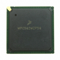
MPC562MZP56 Freescale Semiconductor, MPC562MZP56 Datasheet - Page 421

MPC562MZP56
Manufacturer Part Number
MPC562MZP56
Description
IC MPU 32BIT 56MHZ PPC 388-PBGA
Manufacturer
Freescale Semiconductor
Series
MPC5xxr
Datasheet
1.MPC561MZP56.pdf
(1420 pages)
Specifications of MPC562MZP56
Core Processor
PowerPC
Core Size
32-Bit
Speed
56MHz
Connectivity
CAN, EBI/EMI, SCI, SPI, UART/USART
Peripherals
POR, PWM, WDT
Number Of I /o
64
Program Memory Type
ROMless
Ram Size
32K x 8
Voltage - Supply (vcc/vdd)
2.5 V ~ 2.7 V
Data Converters
A/D 32x10b
Oscillator Type
External
Operating Temperature
-40°C ~ 125°C
Package / Case
388-BGA
Processor Series
MPC5xx
Core
PowerPC
Data Bus Width
32 bit
Data Ram Size
8 KB
Interface Type
SCI, SPI, UART
Maximum Clock Frequency
40 MHz
Number Of Programmable I/os
56
Number Of Timers
22
Operating Supply Voltage
2.6 V to 5 V
Maximum Operating Temperature
+ 85 C
Mounting Style
SMD/SMT
Minimum Operating Temperature
- 40 C
On-chip Adc
2 (10 bit, 32 Channel)
For Use With
MPC564EVB - KIT EVAL FOR MPC561/562/563/564
Lead Free Status / RoHS Status
Request inventory verification / Request inventory verification
Eeprom Size
-
Program Memory Size
-
Lead Free Status / Rohs Status
No
Available stocks
Company
Part Number
Manufacturer
Quantity
Price
Company:
Part Number:
MPC562MZP56
Manufacturer:
FREESCAL
Quantity:
204
Company:
Part Number:
MPC562MZP56
Manufacturer:
Freescale Semiconductor
Quantity:
10 000
Part Number:
MPC562MZP56
Manufacturer:
FREESCALE
Quantity:
20 000
Company:
Part Number:
MPC562MZP56R2
Manufacturer:
RFT
Quantity:
1 441
Company:
Part Number:
MPC562MZP56R2
Manufacturer:
Freescale Semiconductor
Quantity:
10 000
- Current page: 421 of 1420
- Download datasheet (11Mb)
Note: Timing in this table refers to the typical timing only. Consult the electrical characteristics for exact worst-case timing values.
Additional timing rules not covered in
Freescale Semiconductor
•
•
•
•
•
•
TRLX
1/4 clock actually means 0 to 1/4 clock, 1/2 clock means 1/4 to 1/2 clock.
0
1
1
1
1
1
1
1
1
1
If SETA = 1, an external TA signal is required to terminate the cycle.
If TRLX = 1 and SETA = 1, the minimum cycle length = 3 clock cycles (even if SCY = 0000)
If TRLX = 1, the number of wait states = 2 ∗ SCY & 2 ∗ BSCY
ACS = 01 is not defined (reserved).
If EHTR = 1, an extra (idle) clock cycle is inserted between a read cycle and a following read cycle
to another region, or between a read cycle and a following write cycle to any region.
If LBDIP = 1 (late BDIP assertion), the BDIP signal is asserted only after the number of wait states
for the first beat in a burst have elapsed. See
as well as
Access
Type
write
write
write
write
write
write
write
read
read
read
The LBDIP/TBDIP function can operate only when the cycle termination is
internal, using the number of wait states programmed in one of the ORx
registers. The LBDIP/TBDIP function cannot be activated at the same
time—results are unknown.
Section 9.5.5, “Burst
ACS
11
00
10
11
00
10
11
00
10
11
Table 10-3. Programming Rules for Timing Strobes (continued)
CSNT
X
X
X
1
0
0
0
1
1
1
MPC561/MPC563 Reference Manual, Rev. 1.2
1/2 * clock
(1 + 1/4) *
(1 + 1/2) *
(1 + 1/4) *
(1 + 1/2) *
(1 + 1/4) *
(1 + 1/2) *
Asserted
Address
to CS
clock
clock
clock
clock
clock
clock
0
0
0
Table 10-3
Mechanism.”
Negated to
1/2 * clock
1/4 * clock
1/4 * clock
1/4 * clock
1/4 * clock
1/4 * clock
1/4 * clock
1/4 * clock
Add/Data
(1 + 1/2) *
(1 + 1/2) *
Invalid
clock
clock
CS
NOTE
include the following:
Figure 9-13
Address to
WE/BE or
3/4 * clock
(1 + 3/4) *
(1 + 3/4) *
(1 + 3/4) *
Asserted
3/4 clock
3/4 clock
3/4 clock
(1 + 3/4)
(1 + 3/4)
(1 + 3/4)
clock
clock
clock
clock
clock
clock
OE
in
Chapter 9, “External Bus
Negated to
1/2 * clock
1/4 * clock
1/4 * clock
1/4 * clock
Add/Data
(1 + 1/2) *
(1 + 1/2) *
(1 + 1/2) *
WE/BE
Invalid
clock
clock
clock
X
X
X
Negated to
1/4 * clock
1/4 * clock
1/4 * clock
Add/Data
Invalid
OE
X
X
X
X
X
X
X
Memory Controller
Number of
2 + SCY
2 * SCY
2 * SCY
2 * SCY
2 * SCY
2 * SCY
2 * SCY
2 * SCY
2 * SCY
2 * SCY
Cycles
Interface,”
Total
2 +
3 +
3 +
2 +
3 +
3 +
3 +
4 +
4 +
10-23
Related parts for MPC562MZP56
Image
Part Number
Description
Manufacturer
Datasheet
Request
R
Part Number:
Description:
Mpc562 32 Bit Powerpc Microcontroller
Manufacturer:
Freescale Semiconductor, Inc
Datasheet:

Part Number:
Description:
MPC5 1K0 5%
Manufacturer:
TE Connectivity
Datasheet:

Part Number:
Description:
MPC5 500R 5%
Manufacturer:
TE Connectivity
Datasheet:

Part Number:
Description:
MPC5 5K0 5%
Manufacturer:
Tyco Electronics
Datasheet:

Part Number:
Description:
MPC5 5R0 5%
Manufacturer:
Tyco Electronics
Datasheet:

Part Number:
Description:
MPC5 50K 5%
Manufacturer:
Tyco Electronics
Datasheet:
Part Number:
Description:
Manufacturer:
Freescale Semiconductor, Inc
Datasheet:
Part Number:
Description:
Manufacturer:
Freescale Semiconductor, Inc
Datasheet:
Part Number:
Description:
Manufacturer:
Freescale Semiconductor, Inc
Datasheet:
Part Number:
Description:
Manufacturer:
Freescale Semiconductor, Inc
Datasheet:
Part Number:
Description:
Manufacturer:
Freescale Semiconductor, Inc
Datasheet:


