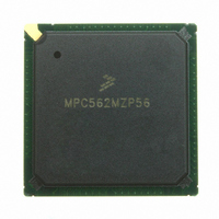
MPC562MZP56 Freescale Semiconductor, MPC562MZP56 Datasheet - Page 422

MPC562MZP56
Manufacturer Part Number
MPC562MZP56
Description
IC MPU 32BIT 56MHZ PPC 388-PBGA
Manufacturer
Freescale Semiconductor
Series
MPC5xxr
Datasheet
1.MPC561MZP56.pdf
(1420 pages)
Specifications of MPC562MZP56
Core Processor
PowerPC
Core Size
32-Bit
Speed
56MHz
Connectivity
CAN, EBI/EMI, SCI, SPI, UART/USART
Peripherals
POR, PWM, WDT
Number Of I /o
64
Program Memory Type
ROMless
Ram Size
32K x 8
Voltage - Supply (vcc/vdd)
2.5 V ~ 2.7 V
Data Converters
A/D 32x10b
Oscillator Type
External
Operating Temperature
-40°C ~ 125°C
Package / Case
388-BGA
Processor Series
MPC5xx
Core
PowerPC
Data Bus Width
32 bit
Data Ram Size
8 KB
Interface Type
SCI, SPI, UART
Maximum Clock Frequency
40 MHz
Number Of Programmable I/os
56
Number Of Timers
22
Operating Supply Voltage
2.6 V to 5 V
Maximum Operating Temperature
+ 85 C
Mounting Style
SMD/SMT
Minimum Operating Temperature
- 40 C
On-chip Adc
2 (10 bit, 32 Channel)
For Use With
MPC564EVB - KIT EVAL FOR MPC561/562/563/564
Lead Free Status / RoHS Status
Request inventory verification / Request inventory verification
Eeprom Size
-
Program Memory Size
-
Lead Free Status / Rohs Status
No
Available stocks
Company
Part Number
Manufacturer
Quantity
Price
Company:
Part Number:
MPC562MZP56
Manufacturer:
FREESCAL
Quantity:
204
Company:
Part Number:
MPC562MZP56
Manufacturer:
Freescale Semiconductor
Quantity:
10 000
Part Number:
MPC562MZP56
Manufacturer:
FREESCALE
Quantity:
20 000
Company:
Part Number:
MPC562MZP56R2
Manufacturer:
RFT
Quantity:
1 441
Company:
Part Number:
MPC562MZP56R2
Manufacturer:
Freescale Semiconductor
Quantity:
10 000
- Current page: 422 of 1420
- Download datasheet (11Mb)
Memory Controller
10.4
The GPCM determines the timing and value of the WE/BE signals if allowed by the port size of the
accessed bank, the transfer size of the transaction and the address accessed.
The functionality of the WE/BE[0:3] signals depends upon the value of the write enable/byte select
(WEBS) bit in the corresponding BR register. Setting WEBS to 1 will enable these signals as BE, while
clearing it to zero will enable them as WE. WE is asserted only during write access, while BE is asserted
for both read and write accesses. The timing of the WE/BE signals remains the same in either case, and is
determined by the TRLX, ACS and CSNT bits.
The upper WE/BE (WE0/BE0) indicates that the upper eight bits of the data bus (D0–D7) contains valid
data during a write/read cycle. The upper-middle write byte enable (WE1/BE1) indicates that the
upper-middle eight bits of the data bus (D8–D15) contains valid data during a write/read cycle. The
lower-middle write byte enable (WE2/BE2) indicates that the lower-middle eight bits of the data bus
(D16–D23) contains valid data during a write/read cycle. The lower write/read enable (WE3/BE3)
indicates that the lower eight bits of the data bus contains valid data during a write cycle.
The write/byte enable lines affected in a transaction for 32-bit port (PS = 00), a 16-bit port (PS = 10) and
a 8-bit port (PS = 01) are shown in
10.5
The internal Flash EEPROM (UC3F) module can be mapped to an external memory region controlled by
the memory controller. Only one region can be programmed to be dual-mapped. When dual mapping is
enabled (DME bit is set in the DMBR register) and when an internal address matches the dual-mapped
address range (as programmed in the DMBR) with the cycle type matching the AT/ATM field in
DMBR/DMOR registers, the following occurs:
10-24
1
•
•
Transfer
Word
Word
This table shows which write enables are asserted (indicated with an ‘X’) for different combinations of port size and
transfer size.
Byte
Half-
Size
The internal Flash memory does not respond to that address
The memory controller takes control of the external access
Write and Byte Enable Signals
Dual Mapping of the Internal Flash EEPROM Array
0
0
0
0
1
1
0
TSIZ
1
1
1
1
0
0
0
A30 A31
Address
0
0
1
1
0
1
0
Table 10-4. Write Enable/Byte Enable Signals Function
0
1
0
1
0
0
0
WE0/
BE0
X
X
X
MPC561/MPC563 Reference Manual, Rev. 1.2
32-bit Port Size
Table
WE1/
BE1
X
X
X
10-4.
WE2
BE2
X
X
X
WE3/
BE3
X
X
X
WE0/
BE0
X
X
X
X
X
16-bit Port Size
WE1/
BE1
X
X
X
X
X
WE2/
BE2
WE3/
BE3
1
WE0
BE0
X
X
X
X
X
X
X
/
8-bit Port Size
Freescale Semiconductor
/BE1
WE1
BE2
WE
2
WE3/
BE3
Related parts for MPC562MZP56
Image
Part Number
Description
Manufacturer
Datasheet
Request
R
Part Number:
Description:
Mpc562 32 Bit Powerpc Microcontroller
Manufacturer:
Freescale Semiconductor, Inc
Datasheet:

Part Number:
Description:
MPC5 1K0 5%
Manufacturer:
TE Connectivity
Datasheet:

Part Number:
Description:
MPC5 500R 5%
Manufacturer:
TE Connectivity
Datasheet:

Part Number:
Description:
MPC5 5K0 5%
Manufacturer:
Tyco Electronics
Datasheet:

Part Number:
Description:
MPC5 5R0 5%
Manufacturer:
Tyco Electronics
Datasheet:

Part Number:
Description:
MPC5 50K 5%
Manufacturer:
Tyco Electronics
Datasheet:
Part Number:
Description:
Manufacturer:
Freescale Semiconductor, Inc
Datasheet:
Part Number:
Description:
Manufacturer:
Freescale Semiconductor, Inc
Datasheet:
Part Number:
Description:
Manufacturer:
Freescale Semiconductor, Inc
Datasheet:
Part Number:
Description:
Manufacturer:
Freescale Semiconductor, Inc
Datasheet:
Part Number:
Description:
Manufacturer:
Freescale Semiconductor, Inc
Datasheet:


