MPC562MZP56 Freescale Semiconductor, MPC562MZP56 Datasheet - Page 652
MPC562MZP56
Manufacturer Part Number
MPC562MZP56
Description
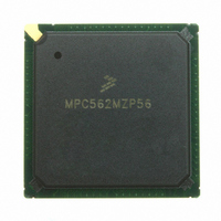
IC MPU 32BIT 56MHZ PPC 388-PBGA
Manufacturer
Freescale Semiconductor
Series
MPC5xxr
Datasheet
1.MPC561MZP56.pdf
(1420 pages)
Specifications of MPC562MZP56
Core Processor
PowerPC
Core Size
32-Bit
Speed
56MHz
Connectivity
CAN, EBI/EMI, SCI, SPI, UART/USART
Peripherals
POR, PWM, WDT
Number Of I /o
64
Program Memory Type
ROMless
Ram Size
32K x 8
Voltage - Supply (vcc/vdd)
2.5 V ~ 2.7 V
Data Converters
A/D 32x10b
Oscillator Type
External
Operating Temperature
-40°C ~ 125°C
Package / Case
388-BGA
Processor Series
MPC5xx
Core
PowerPC
Data Bus Width
32 bit
Data Ram Size
8 KB
Interface Type
SCI, SPI, UART
Maximum Clock Frequency
40 MHz
Number Of Programmable I/os
56
Number Of Timers
22
Operating Supply Voltage
2.6 V to 5 V
Maximum Operating Temperature
+ 85 C
Mounting Style
SMD/SMT
Minimum Operating Temperature
- 40 C
On-chip Adc
2 (10 bit, 32 Channel)
For Use With
MPC564EVB - KIT EVAL FOR MPC561/562/563/564
Lead Free Status / RoHS Status
Request inventory verification / Request inventory verification
Eeprom Size
-
Program Memory Size
-
Lead Free Status / Rohs Status
No
Available stocks
Company
Part Number
Manufacturer
Quantity
Price
Company:

Part Number:
MPC562MZP56
Manufacturer:
FREESCAL
Quantity:
204
Company:
Part Number:
MPC562MZP56
Manufacturer:
Freescale Semiconductor
Quantity:
10 000
Part Number:
MPC562MZP56
Manufacturer:
FREESCALE
Quantity:
20 000
Company:
Part Number:
MPC562MZP56R2
Manufacturer:
RFT
Quantity:
1 441
Company:
Part Number:
MPC562MZP56R2
Manufacturer:
Freescale Semiconductor
Quantity:
10 000


Queued Serial Multi-Channel Module
Normally, the SPI bus performs synchronous bidirectional transfers. The serial clock on the SPI bus master
supplies the clock signal SCK to time the transfer of data. Four possible combinations of clock phase and
polarity can be specified by the CPHA and CPOL bits in SPCR0.
Data is transferred with the most significant bit first. The number of bits transferred per command defaults
to eight, but can be set to any value from eight to sixteen bits by writing a value into the BITS field in
SPCR0 and setting BITSE in command RAM.
Typically, SPI bus outputs are not open drain unless multiple SPI masters are in the system. If needed, the
WOMQ bit in SPCR0 can be set to provide wired-OR, open drain outputs. An external pull-up resistor
should be used on each output line. WOMQ affects all QSPI pins regardless of whether they are assigned
to the QSPI or used as general-purpose I/O.
15.6.5
Master Mode Operation
Setting the MSTR bit in SPCR0 selects master mode operation. In master mode, the QSPI can initiate serial
transfers, but cannot respond to externally initiated transfers. When the slave select input of a device
configured for master mode is asserted, a mode fault occurs.
Before QSPI operation begins, PQSPAR must be written to assign the necessary pins to the QSPI. The pins
necessary for master mode operation are MISO, MOSI, SCK, and one or more of the chip-select pins.
MISO is used for serial data input in master mode, and MOSI is used for serial data output. Either or both
may be necessary, depending on the particular application. SCK is the serial clock output in master mode
and must be assigned to the QSPI for proper operation.
The PORTQS data register must next be written with values that make the QGPIO6/SCK (bit 13 QDSCK
of PORTQS) and QGPIO[3:0]/PCS[3:0] (bits 12:9 QDPCS[3:0] of PORTQS) outputs inactive when the
QSPI completes a series of transfers. Pins allocated to the QSPI by PQSPAR are controlled by PORTQS
when the QSPI is inactive. PORTQS I/O pins driven to states opposite those of the inactive QSPI signals
can generate glitches that momentarily enable or partially clock a slave device.
For example, if a slave device operates with an inactive SCK state of logic one (CPOL = 1) and uses active
low peripheral chip-select PCS0, the QDSCK and QDPCS0 bits in PORTQS must be set to 0b11. If
QDSCK and QDPCS0 = 0b00, falling edges will appear on QGPIO6/SCK and GPIO0/PCS0 as the QSPI
relinquishes control of these pins and PORTQS drives them to logic zero from the inactive SCK and PCS0
states of logic one.
Before master mode operation is initiated, QSMCM register DDRQS is written last to direct the data flow
on the QSPI pins used. Configure the SCK, MOSI and appropriate chip-select pins PCS[3:0] as outputs.
The MISO pin must be configured as an input.
After pins are assigned and configured, write appropriate data to the command queue. If data is to be
transmitted, write the data to transmit RAM. Initialize the queue pointers as appropriate.
QSPI operation is initiated by setting the SPE bit in SPCR1. Shortly after SPE is set, the QSPI executes
the command at the command RAM address pointed to by NEWQP. Data at the pointer address in transmit
RAM is loaded into the data serializer and transmitted. Data that is simultaneously received is stored at the
pointer address in receive RAM.
MPC561/MPC563 Reference Manual, Rev. 1.2
15-34
Freescale Semiconductor
Related parts for MPC562MZP56
Image
Part Number
Description
Manufacturer
Datasheet
Request
R

Part Number:
Description:
Mpc562 32 Bit Powerpc Microcontroller
Manufacturer:
Freescale Semiconductor, Inc
Datasheet:

Part Number:
Description:
MPC5 1K0 5%
Manufacturer:
TE Connectivity
Datasheet:


Part Number:
Description:
MPC5 500R 5%
Manufacturer:
TE Connectivity
Datasheet:

Part Number:
Description:
MPC5 5K0 5%
Manufacturer:
Tyco Electronics
Datasheet:
Part Number:
Description:
MPC5 5R0 5%
Manufacturer:
Tyco Electronics
Datasheet:
Part Number:
Description:
MPC5 50K 5%
Manufacturer:
Tyco Electronics
Datasheet:
Part Number:
Description:
Manufacturer:
Freescale Semiconductor, Inc
Datasheet:
Part Number:
Description:
Manufacturer:
Freescale Semiconductor, Inc
Datasheet:
Part Number:
Description:
Manufacturer:
Freescale Semiconductor, Inc
Datasheet:
Part Number:
Description:
Manufacturer:
Freescale Semiconductor, Inc
Datasheet:
Part Number:
Description:
Manufacturer:
Freescale Semiconductor, Inc
Datasheet: