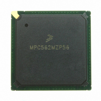
MPC562MZP56 Freescale Semiconductor, MPC562MZP56 Datasheet - Page 655

MPC562MZP56
Manufacturer Part Number
MPC562MZP56
Description
IC MPU 32BIT 56MHZ PPC 388-PBGA
Manufacturer
Freescale Semiconductor
Series
MPC5xxr
Datasheet
1.MPC561MZP56.pdf
(1420 pages)
Specifications of MPC562MZP56
Core Processor
PowerPC
Core Size
32-Bit
Speed
56MHz
Connectivity
CAN, EBI/EMI, SCI, SPI, UART/USART
Peripherals
POR, PWM, WDT
Number Of I /o
64
Program Memory Type
ROMless
Ram Size
32K x 8
Voltage - Supply (vcc/vdd)
2.5 V ~ 2.7 V
Data Converters
A/D 32x10b
Oscillator Type
External
Operating Temperature
-40°C ~ 125°C
Package / Case
388-BGA
Processor Series
MPC5xx
Core
PowerPC
Data Bus Width
32 bit
Data Ram Size
8 KB
Interface Type
SCI, SPI, UART
Maximum Clock Frequency
40 MHz
Number Of Programmable I/os
56
Number Of Timers
22
Operating Supply Voltage
2.6 V to 5 V
Maximum Operating Temperature
+ 85 C
Mounting Style
SMD/SMT
Minimum Operating Temperature
- 40 C
On-chip Adc
2 (10 bit, 32 Channel)
For Use With
MPC564EVB - KIT EVAL FOR MPC561/562/563/564
Lead Free Status / RoHS Status
Request inventory verification / Request inventory verification
Eeprom Size
-
Program Memory Size
-
Lead Free Status / Rohs Status
No
Available stocks
Company
Part Number
Manufacturer
Quantity
Price
Company:
Part Number:
MPC562MZP56
Manufacturer:
FREESCAL
Quantity:
204
Company:
Part Number:
MPC562MZP56
Manufacturer:
Freescale Semiconductor
Quantity:
10 000
Part Number:
MPC562MZP56
Manufacturer:
FREESCALE
Quantity:
20 000
Company:
Part Number:
MPC562MZP56R2
Manufacturer:
RFT
Quantity:
1 441
Company:
Part Number:
MPC562MZP56R2
Manufacturer:
Freescale Semiconductor
Quantity:
10 000
- Current page: 655 of 1420
- Download datasheet (11Mb)
Delay after transfer can be used to provide a peripheral deselect interval. A delay can also be inserted
between consecutive transfers to allow serial A/D converters to complete conversion.
Adequate delay between transfers must be specified for long data streams because the QSPI requires time
to load a transmit RAM entry for transfer. Receiving devices need at least the standard delay between
successive transfers. If the IMB3 clock is operating at a slower rate, the delay between transfers must be
increased proportionately.
15.6.5.5
There are two transfer length options. The user can choose a default value of eight bits, or a programmed
value from eight (0b1000) to 16 (0b0000) bits, inclusive. Reserved values (from 0b0001 to 0b0111) default
to eight bits. The programmed value must be written into the BITS field in SPCR0. The BITSE bit in each
command RAM byte determines whether the default value (BITSE = 0) or the BITS value (BITSE = 1) is
used.
15.6.5.6
Peripheral chip-select signals are used to select an external device for serial data transfer. Chip-select
signals are asserted when a command in the queue is executed. Signals are asserted at a logic level
corresponding to the value of the PCS[3:0] bits in each command byte. More than one chip-select signal
can be asserted at a time, and more than one external device can be connected to the PCS pins, provided
proper fanout is observed. PCS0 shares a pin with the slave select SS signal, which initiates slave mode
serial transfer. If SS is taken low when the QSPI is in master mode, a mode fault occurs.
To configure a peripheral chip select, set the appropriate bit in the PQSPAR, then configure the chip-select
pin as an output by setting the appropriate bit in DDRQS. The value of the bit in PORTQS that corresponds
to the chip-select pin determines the base state of the chip-select signal. If the base state is zero, chip-select
assertion must be active high (PCS bit in command RAM must be set); if base state is one, assertion must
be active low (PCS bit in command RAM must be cleared). PORTQS bits are cleared during reset. If no
new data is written to PORTQS before pin assignment and configuration as an output, the base state of
chip-select signals is zero and chip-select pins are configured for active-high operation.
15.6.5.7
The MPC561/MPC563 have an optional on-chip decoder for the peripheral chip selects. It is enabled if
any of the PCS[4:7]EN bits are enabled in the PDMCR2 register (see
normal PCS[0:3] chip selects into a 1 of 8 decode. The polarity of the new PCS outputs can be selected by
the state of the PCSV bit in the PDMCR2. See
Freescale Semiconductor
Transfer Length
Peripheral Chip Selects
Optional Enhanced Peripheral Chip Selects
PCS_IN[3:0]
0000
0001
0010
Table 15-22. PCS Enhanced Functionality
MPC561/MPC563 Reference Manual, Rev. 1.2
PCS_OUT[7:0] IF PCSV = 0
00000001
00000010
00000100
Table
15-22.
Table
PCS_OUT[7:0] IF PCSV = 1
2-6). The decode translates the
Queued Serial Multi-Channel Module
11111110
11111101
11111011
15-37
Related parts for MPC562MZP56
Image
Part Number
Description
Manufacturer
Datasheet
Request
R
Part Number:
Description:
Mpc562 32 Bit Powerpc Microcontroller
Manufacturer:
Freescale Semiconductor, Inc
Datasheet:

Part Number:
Description:
MPC5 1K0 5%
Manufacturer:
TE Connectivity
Datasheet:

Part Number:
Description:
MPC5 500R 5%
Manufacturer:
TE Connectivity
Datasheet:

Part Number:
Description:
MPC5 5K0 5%
Manufacturer:
Tyco Electronics
Datasheet:

Part Number:
Description:
MPC5 5R0 5%
Manufacturer:
Tyco Electronics
Datasheet:

Part Number:
Description:
MPC5 50K 5%
Manufacturer:
Tyco Electronics
Datasheet:
Part Number:
Description:
Manufacturer:
Freescale Semiconductor, Inc
Datasheet:
Part Number:
Description:
Manufacturer:
Freescale Semiconductor, Inc
Datasheet:
Part Number:
Description:
Manufacturer:
Freescale Semiconductor, Inc
Datasheet:
Part Number:
Description:
Manufacturer:
Freescale Semiconductor, Inc
Datasheet:
Part Number:
Description:
Manufacturer:
Freescale Semiconductor, Inc
Datasheet:


