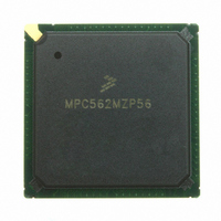
MPC562MZP56 Freescale Semiconductor, MPC562MZP56 Datasheet - Page 782

MPC562MZP56
Manufacturer Part Number
MPC562MZP56
Description
IC MPU 32BIT 56MHZ PPC 388-PBGA
Manufacturer
Freescale Semiconductor
Series
MPC5xxr
Datasheet
1.MPC561MZP56.pdf
(1420 pages)
Specifications of MPC562MZP56
Core Processor
PowerPC
Core Size
32-Bit
Speed
56MHz
Connectivity
CAN, EBI/EMI, SCI, SPI, UART/USART
Peripherals
POR, PWM, WDT
Number Of I /o
64
Program Memory Type
ROMless
Ram Size
32K x 8
Voltage - Supply (vcc/vdd)
2.5 V ~ 2.7 V
Data Converters
A/D 32x10b
Oscillator Type
External
Operating Temperature
-40°C ~ 125°C
Package / Case
388-BGA
Processor Series
MPC5xx
Core
PowerPC
Data Bus Width
32 bit
Data Ram Size
8 KB
Interface Type
SCI, SPI, UART
Maximum Clock Frequency
40 MHz
Number Of Programmable I/os
56
Number Of Timers
22
Operating Supply Voltage
2.6 V to 5 V
Maximum Operating Temperature
+ 85 C
Mounting Style
SMD/SMT
Minimum Operating Temperature
- 40 C
On-chip Adc
2 (10 bit, 32 Channel)
For Use With
MPC564EVB - KIT EVAL FOR MPC561/562/563/564
Lead Free Status / RoHS Status
Request inventory verification / Request inventory verification
Eeprom Size
-
Program Memory Size
-
Lead Free Status / Rohs Status
No
Available stocks
Company
Part Number
Manufacturer
Quantity
Price
Company:
Part Number:
MPC562MZP56
Manufacturer:
FREESCAL
Quantity:
204
Company:
Part Number:
MPC562MZP56
Manufacturer:
Freescale Semiconductor
Quantity:
10 000
Part Number:
MPC562MZP56
Manufacturer:
FREESCALE
Quantity:
20 000
Company:
Part Number:
MPC562MZP56R2
Manufacturer:
RFT
Quantity:
1 441
Company:
Part Number:
MPC562MZP56R2
Manufacturer:
Freescale Semiconductor
Quantity:
10 000
- Current page: 782 of 1420
- Download datasheet (11Mb)
Modular Input/Output Subsystem (MIOS14)
The relationship between the output frequency obtained (F
(f
loaded in the counter (V
17.10.3.4 Pulse Width Registers
The pulse width section is composed of two 16-bit data registers (MPWMPULR1 and MPWMPULR2).
Only MPWMPULR1 is accessible by software. The software establishes the pulse width of the
MPWMSM output signal in MPWMPULR1. MPWMPULR2 is used as a double buffer of
MPWMPULR1.
When the MPWMSM is running in transparent mode, the pulse width value in MPWMPULR1 is
immediately transferred in MPWMPULR2 so that the new value takes effect immediately.
When the MPWMSM is not running in double-buffered mode, the pulse width value in MPWMPULR1
can be changed at any time without affecting the current pulse width of the output signal. The new value
in MPWMPULR1 will be transferred to MPWMPULR2 only when the down-counter reaches the value of
0x0001.
When the counter first reaches the value in MPWMPULR2, the output flip-flop is set. The output is reset
when the counter reaches 0x0001. The pulse width match starts the width of the output signal, it does not
affect the counter. MPWMPULR1 is software readable and writable at any time. The MPWMSM does not
modify the content of MPWMPULR1.
The PWM output pulse width can be as wide as one period minus one MPWMSM clock count: (i.e.,
MPWMPULR2 = MPWMPERR — [one MPWMSM clock count]). At the other end of the pulse width
range, MPWMPULR2 can contain 0x0001 to create a pulse width of one PWM clock count.
17-50
SYS
•
•
•
), the MCPSM clock divide ratio (N
The value 0x0000 in the period register, causes the counter to act like a free running counter. This
condition creates a period of 65536 PWM clock periods.
The value 0x0001 in the period register will always cause a period match to occur and the counter
will never decrement below 0x0001. This condition is defined as a period of “1” PWM clock count.
The output flip-flop is always set unless MPWMPULR = 0x0000, when the output flip-flop is
always reset. Refer to
100% duty cycles.
Writing value 0x0002 in the period register causes a period match to occur every two clock periods.
The counter decrements from 0x0002 to 0x0001, and then it is initialized back to 0x0002. This
condition is defined as a period of 2 clock counts. Note that the value 0x0002 loaded in the period
register and a value of 0x0001 in the pulse width register is the condition to obtain the maximum
possible output frequency for a given clock period.
When the MPWMSM is in disable mode, writing to MPWMPULR1 will
write automatically to MPWMPULR2.
COUNTER
f
PWMO
Section 17.10.3.5, “Duty Cycles (0% and
MPC561/MPC563 Reference Manual, Rev. 1.2
=
) is given by the following equation:
MCPSM
N
MCPSM
), the counter divide ratio (N
NOTE
• N
MPWMSM
f
SYS
PWMO
• V
COUNTER
) and the MIOS14 CLOCK frequency
100%)” for details about 0% and
MPWMSM
Freescale Semiconductor
) and the value
Related parts for MPC562MZP56
Image
Part Number
Description
Manufacturer
Datasheet
Request
R
Part Number:
Description:
Mpc562 32 Bit Powerpc Microcontroller
Manufacturer:
Freescale Semiconductor, Inc
Datasheet:

Part Number:
Description:
MPC5 1K0 5%
Manufacturer:
TE Connectivity
Datasheet:

Part Number:
Description:
MPC5 500R 5%
Manufacturer:
TE Connectivity
Datasheet:

Part Number:
Description:
MPC5 5K0 5%
Manufacturer:
Tyco Electronics
Datasheet:

Part Number:
Description:
MPC5 5R0 5%
Manufacturer:
Tyco Electronics
Datasheet:

Part Number:
Description:
MPC5 50K 5%
Manufacturer:
Tyco Electronics
Datasheet:
Part Number:
Description:
Manufacturer:
Freescale Semiconductor, Inc
Datasheet:
Part Number:
Description:
Manufacturer:
Freescale Semiconductor, Inc
Datasheet:
Part Number:
Description:
Manufacturer:
Freescale Semiconductor, Inc
Datasheet:
Part Number:
Description:
Manufacturer:
Freescale Semiconductor, Inc
Datasheet:
Part Number:
Description:
Manufacturer:
Freescale Semiconductor, Inc
Datasheet:


