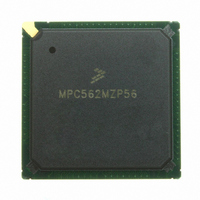
MPC562MZP56 Freescale Semiconductor, MPC562MZP56 Datasheet - Page 875

MPC562MZP56
Manufacturer Part Number
MPC562MZP56
Description
IC MPU 32BIT 56MHZ PPC 388-PBGA
Manufacturer
Freescale Semiconductor
Series
MPC5xxr
Datasheet
1.MPC561MZP56.pdf
(1420 pages)
Specifications of MPC562MZP56
Core Processor
PowerPC
Core Size
32-Bit
Speed
56MHz
Connectivity
CAN, EBI/EMI, SCI, SPI, UART/USART
Peripherals
POR, PWM, WDT
Number Of I /o
64
Program Memory Type
ROMless
Ram Size
32K x 8
Voltage - Supply (vcc/vdd)
2.5 V ~ 2.7 V
Data Converters
A/D 32x10b
Oscillator Type
External
Operating Temperature
-40°C ~ 125°C
Package / Case
388-BGA
Processor Series
MPC5xx
Core
PowerPC
Data Bus Width
32 bit
Data Ram Size
8 KB
Interface Type
SCI, SPI, UART
Maximum Clock Frequency
40 MHz
Number Of Programmable I/os
56
Number Of Timers
22
Operating Supply Voltage
2.6 V to 5 V
Maximum Operating Temperature
+ 85 C
Mounting Style
SMD/SMT
Minimum Operating Temperature
- 40 C
On-chip Adc
2 (10 bit, 32 Channel)
For Use With
MPC564EVB - KIT EVAL FOR MPC561/562/563/564
Lead Free Status / RoHS Status
Request inventory verification / Request inventory verification
Eeprom Size
-
Program Memory Size
-
Lead Free Status / Rohs Status
No
Available stocks
Company
Part Number
Manufacturer
Quantity
Price
Company:
Part Number:
MPC562MZP56
Manufacturer:
FREESCAL
Quantity:
204
Company:
Part Number:
MPC562MZP56
Manufacturer:
Freescale Semiconductor
Quantity:
10 000
Part Number:
MPC562MZP56
Manufacturer:
FREESCALE
Quantity:
20 000
Company:
Part Number:
MPC562MZP56R2
Manufacturer:
RFT
Quantity:
1 441
Company:
Part Number:
MPC562MZP56R2
Manufacturer:
Freescale Semiconductor
Quantity:
10 000
- Current page: 875 of 1420
- Download datasheet (11Mb)
Freescale Semiconductor
16:23
26:27
Bits
24
25
28
29
BLOCK
Name
HSUS
CSC
PE
—
—
Block program and erase select. The BLOCK bits are write protected by the SES bit. BLOCK
selects the UC3F EEPROM array blocks for program and erase operation. All the blocks may be
selected for program or erase operation at once.
The UC3F EEPROM configuration along with BLOCK determine which array blocks that may be
programmed. The UC3F EEPROM array blocks that are enabled to be programmed by the
program operation are the blocks whose corresponding BLOCK bit is set to 1. For example, if
array blocks 2 and 5 are enabled for programming, BLOCK[2] and BLOCK[5] must be set to 1
while BLOCK[0], BLOCK[1], BLOCK[3], BLOCK[4], BLOCK[6], and BLOCK[7] are set to 0.
The UC3F EEPROM configuration along with BLOCK determine the blocks that will be erased
simultaneously. All array blocks whose corresponding BLOCK bits are set will be erased during
the erase operation. For example, if BLOCK = 00100111, then array blocks 2, 5, 6, and 7 get
erased when an erase operation is performed.
0 Array block M is not selected for program or erase
1 Array block M is selected for program or erase
Reserved
Censor set or clear. The CSC bit is write protected by the SES bit. CSC configures the UC3F
EEPROM for setting or clearing CENSOR. If CSC = 1 then CENSOR is configured for setting if
PE = 0 or clearing if PE = 1.
When the CSC bit is set, the following bits in the UC3FMCR register are write-locked: LOCK,
FIC, ACCESS, SUPV, DATA, and PROTECT.
0 Configure for normal operation
1 Configure to set or clear the CENSOR bits
Reserved
Program/erase suspend. Setting the HSUS bit during an embedded hardware algorithm
program or erase operation will force the UC3F EEPROM to suspend the current program or
erase. The UC3F EEPROM will maintain all information necessary to resume the suspended
operation.
Array reads are possible while HSUS = 1. However, array reads must be done to locations that
are not being affected by the program/erase operation that is currently being suspended. The
UC3F EEPROM will NOT prevent read accesses to those locations. Reads to those locations
will result in UNKNOWN data. Writes to the HSUS bit only have effect while EHV = 1. The HSUS
bit is write locked by EHV = 0.
0 Hardware program/erase behaves normally
1 Any current hardware program/erase is suspended
Program or erase select. The PE bit is write protected by the SES bit. PE configures the UC3F
EEPROM for programming or erasing. When PE = 0, the array is configured for programming
and if SES = 1 the SIE bit will be write locked. When PE = 1, the array is configured for erasing
and SES will not write lock the SIE bit.
0 Configure for program operation
1 Configure for erase operation
Table 21-5. UC3FCTL Bit Descriptions (continued)
MPC561/MPC563 Reference Manual, Rev. 1.2
Description
CDR3 Flash (UC3F) EEPROM
21-13
Related parts for MPC562MZP56
Image
Part Number
Description
Manufacturer
Datasheet
Request
R
Part Number:
Description:
Mpc562 32 Bit Powerpc Microcontroller
Manufacturer:
Freescale Semiconductor, Inc
Datasheet:

Part Number:
Description:
MPC5 1K0 5%
Manufacturer:
TE Connectivity
Datasheet:

Part Number:
Description:
MPC5 500R 5%
Manufacturer:
TE Connectivity
Datasheet:

Part Number:
Description:
MPC5 5K0 5%
Manufacturer:
Tyco Electronics
Datasheet:

Part Number:
Description:
MPC5 5R0 5%
Manufacturer:
Tyco Electronics
Datasheet:

Part Number:
Description:
MPC5 50K 5%
Manufacturer:
Tyco Electronics
Datasheet:
Part Number:
Description:
Manufacturer:
Freescale Semiconductor, Inc
Datasheet:
Part Number:
Description:
Manufacturer:
Freescale Semiconductor, Inc
Datasheet:
Part Number:
Description:
Manufacturer:
Freescale Semiconductor, Inc
Datasheet:
Part Number:
Description:
Manufacturer:
Freescale Semiconductor, Inc
Datasheet:
Part Number:
Description:
Manufacturer:
Freescale Semiconductor, Inc
Datasheet:


