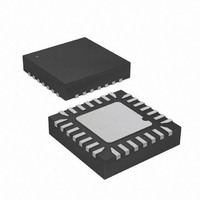
ATMEGA48V-10MMU Atmel, ATMEGA48V-10MMU Datasheet - Page 290

ATMEGA48V-10MMU
Manufacturer Part Number
ATMEGA48V-10MMU
Description
MCU AVR 4K FLASH 10MHZ 28-QFN
Manufacturer
Atmel
Series
AVR® ATmegar
Specifications of ATMEGA48V-10MMU
Core Processor
AVR
Core Size
8-Bit
Speed
10MHz
Connectivity
I²C, SPI, UART/USART
Peripherals
Brown-out Detect/Reset, POR, PWM, WDT
Number Of I /o
23
Program Memory Size
4KB (2K x 16)
Program Memory Type
FLASH
Eeprom Size
256 x 8
Ram Size
512 x 8
Voltage - Supply (vcc/vdd)
1.8 V ~ 5.5 V
Data Converters
A/D 8x10b
Oscillator Type
Internal
Operating Temperature
-40°C ~ 85°C
Package / Case
28-VQFN Exposed Pad, 28-HVQFN, 28-SQFN, 28-DHVQFN
Processor Series
ATMEGA48x
Core
AVR8
Data Bus Width
8 bit
Data Ram Size
512 B
Interface Type
2-Wire, SPI, USART, Serial
Maximum Clock Frequency
10 MHz
Number Of Programmable I/os
23
Number Of Timers
3
Maximum Operating Temperature
+ 85 C
Mounting Style
SMD/SMT
3rd Party Development Tools
EWAVR, EWAVR-BL
Minimum Operating Temperature
- 40 C
On-chip Adc
10 bit, 8 Channel
Package
28MLF EP
Device Core
AVR
Family Name
ATmega
Maximum Speed
10 MHz
Operating Supply Voltage
2.5|3.3|5 V
For Use With
ATSTK600 - DEV KIT FOR AVR/AVR32ATAVRDRAGON - KIT DRAGON 32KB FLASH MEM AVR
Lead Free Status / RoHS Status
Lead free / RoHS Compliant
Available stocks
Company
Part Number
Manufacturer
Quantity
Price
Company:
Part Number:
ATMEGA48V-10MMU
Manufacturer:
ZILOG
Quantity:
1
- Current page: 290 of 378
- Download datasheet (8Mb)
27.7
27.7.1
290
Parallel Programming
ATmega48/88/168
Enter Programming Mode
Table 27-13. XA1 and XA0 Coding
Table 27-14. Command Byte Bit Coding
The following algorithm puts the device in Parallel (High-voltage) Programming mode:
1. Set Prog_enable pins listed in
2. Apply 4.5V - 5.5V between V
Ensure that V
3. Wait 20 µs - 60 µs, and apply 11.5V - 12.5V to RESET.
4. Keep the Prog_enable pins unchanged for at least 10µs after the High-voltage has been
5. Wait at least 300 µs before giving any parallel programming commands.
6. Exit Programming mode by power the device down or by bringing RESET pin to 0V.
If the rise time of the V
tive algorithm can be used.
1. Set Prog_enable pins listed in
2. Apply 4.5V - 5.5V between V
3. Monitor V
Command Byte
XA1
V
applied to ensure the Prog_enable Signature has been latched.
V
0
0
1
1
CC
CC
1000 0000
0100 0000
0010 0000
0001 0000
0001 0001
0000 1000
0000 0100
0000 0010
0000 0011
to 0V.
to 0V.
CC
XA0
CC
0
1
0
1
, and as soon as V
reaches at least 1.8V within the next 20 µs.
Action when XTAL1 is Pulsed
Load Flash or EEPROM Address (High or low address byte determined by BS1).
Load Data (High or Low data byte for Flash determined by BS1).
Load Command
No Action, Idle
Command Executed
Chip Erase
Write Fuse bits
Write Lock bits
Write Flash
Write EEPROM
Read Signature Bytes and Calibration byte
Read Fuse and Lock bits
Read Flash
Read EEPROM
CC
is unable to fulfill the requirements listed above, the following alterna-
CC
CC
Table 27-12 on page 289
Table 27-12 on page 289
CC
and GND.
and GND.
reaches 0.9V - 1.1V, apply 11.5V - 12.5V to RESET.
to “0000”, RESET pin to 0V and
to “0000”, RESET pin to 0V and
2545S–AVR–07/10
Related parts for ATMEGA48V-10MMU
Image
Part Number
Description
Manufacturer
Datasheet
Request
R

Part Number:
Description:
IC AVR MCU 4K 5V 10MHZ 32-TQFP
Manufacturer:
Atmel
Datasheet:

Part Number:
Description:
IC AVR MCU 4K 10MHZ 1.8V 32-QFN
Manufacturer:
Atmel
Datasheet:

Part Number:
Description:
IC AVR MCU 4K 10MHZ 1.8V 28DIP
Manufacturer:
Atmel
Datasheet:

Part Number:
Description:
IC AVR MCU 4K 5V 10MHZ 32-TQFP
Manufacturer:
Atmel
Datasheet:

Part Number:
Description:
IC AVR MCU 4K 5V 12MHZ 32-QFN
Manufacturer:
Atmel
Datasheet:

Part Number:
Description:
IC AVR MCU 4K 5V 10MHZ 32-QFN
Manufacturer:
Atmel
Datasheet:

Part Number:
Description:
IC AVR MCU 4K 5V 10MHZ 28-DIP
Manufacturer:
Atmel
Datasheet:

Part Number:
Description:
IC AVR MCU 4K 5V 10MHZ 28-DIP
Manufacturer:
Atmel
Datasheet:

Part Number:
Description:
MCU AVR 4KB FLASH 10MHZ 32TQFP
Manufacturer:
Atmel
Datasheet:

Part Number:
Description:
MCU AVR 4KB FLASH 10MHZ 32QFN
Manufacturer:
Atmel
Datasheet:

Part Number:
Description:
MCU AVR 4KB FLASH 20MHZ 28QFN
Manufacturer:
Atmel
Datasheet:


