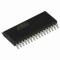
AT90PWM316-16SUR Atmel, AT90PWM316-16SUR Datasheet - Page 75

AT90PWM316-16SUR
Manufacturer Part Number
AT90PWM316-16SUR
Description
MCU AVR 16K FLASH 16MHZ 32-SOIC
Manufacturer
Atmel
Series
AVR® 90PWM Lightingr
Datasheet
1.AT90PWM216-16SU.pdf
(359 pages)
Specifications of AT90PWM316-16SUR
Core Processor
AVR
Core Size
8-Bit
Speed
16MHz
Connectivity
SPI, UART/USART
Peripherals
Brown-out Detect/Reset, POR, PWM, WDT
Number Of I /o
27
Program Memory Size
16KB (16K x 8)
Program Memory Type
FLASH
Eeprom Size
512 x 8
Ram Size
1K x 8
Voltage - Supply (vcc/vdd)
2.7 V ~ 5.5 V
Data Converters
A/D 11x10b; D/A 1x10b
Oscillator Type
Internal
Operating Temperature
-40°C ~ 105°C
Package / Case
32-SOIC (7.5mm Width)
For Use With
ATSTK600-SOIC - STK600 SOCKET/ADAPTER FOR SOICATAVRMC200 - KIT EVAL FOR AT90PWM3 ASYNCATAVRFBKIT - KIT DEMO BALLAST FOR AT90PWM2
Lead Free Status / RoHS Status
Lead free / RoHS Compliant
Available stocks
Company
Part Number
Manufacturer
Quantity
Price
- Current page: 75 of 359
- Download datasheet (6Mb)
7710E–AVR–08/10
CLKO, Divided System Clock: The divided system clock can be output on this pin. The divided
system clock will be output if the CKOUT Fuse is programmed, regardless of the PORTD1 and
DDD1 settings. It will also be output during reset.
• PSCOUT00/XCK/SS_A – Bit 0
PSCOUT00: Output 0 of PSC 0.
XCK, USART External clock. The Data Direction Register (DDD0) controls whether the clock is
output (DDD0 set) or input (DDD0 cleared). The XCK0 pin is active only when the USART oper-
ates in Synchronous mode.
SS_A: Slave Port Select input. When the SPI is enabled as a slave, this pin is configured as an
input regardless of the setting of DDD0. As a slave, the SPI is activated when this pin is driven
low. When the SPI is enabled as a master, the data direction of this pin is controlled by DDD0.
When the pin is forced to be an input, the pull-up can still be controlled by the PORTD0 bit.
Table 11-10
shown in
Table 11-10. Overriding Signals for Alternate Functions PD7..PD4
Signal Name
PUOE
PUOV
DDOE
DDOV
PVOE
PVOV
DIEOE
DIEOV
DI
AIO
Figure 11-5 on page
and
Table 11-11
PD7/
ACMP0
0
0
0
0
0
0
ACMP0D
0
–
ACOMP0
relates the alternate functions of Port D to the overriding signals
65.
PD6/ADC3/
ACMPM/INT0
0
0
0
0
0
0
ADC3D + In0en
In0en
INT0
ADC3
ACMPM
PD5/ADC2/
ACMP2
0
0
0
0
0
ADC2D
0
ADC2
ACOMP2
0
AT90PWM216/316
PD4/ADC1/RXD/
ICP1A/SCK_A
RXEN + SPE •
MSTR • SPIPS
PD4 •
PUD
RXEN + SPE •
MSTR • SPIPS
0
SPE • MSTR •
SPIPS
–
ADC1D
0
ICP1A
ADC1
75
Related parts for AT90PWM316-16SUR
Image
Part Number
Description
Manufacturer
Datasheet
Request
R

Part Number:
Description:
Manufacturer:
Atmel Corporation
Datasheet:

Part Number:
Description:
MCU AVR 16K FLASH 16MHZ 32-QFN
Manufacturer:
Atmel
Datasheet:

Part Number:
Description:
MCU AVR 16K ISP FLSH 16MHZ32SOIC
Manufacturer:
Atmel
Datasheet:

Part Number:
Description:
8-bit Microcontroller with 16K Bytes In-System Programmable Flash
Manufacturer:
ATMEL [ATMEL Corporation]
Datasheet:

Part Number:
Description:
8-bit Avr Microcontroller With 16k Bytes Of Isp Flash And Usb Controller
Manufacturer:
ATMEL Corporation
Datasheet:

Part Number:
Description:
DEV KIT FOR AVR/AVR32
Manufacturer:
Atmel
Datasheet:

Part Number:
Description:
INTERVAL AND WIPE/WASH WIPER CONTROL IC WITH DELAY
Manufacturer:
ATMEL Corporation
Datasheet:

Part Number:
Description:
Low-Voltage Voice-Switched IC for Hands-Free Operation
Manufacturer:
ATMEL Corporation
Datasheet:

Part Number:
Description:
MONOLITHIC INTEGRATED FEATUREPHONE CIRCUIT
Manufacturer:
ATMEL Corporation
Datasheet:

Part Number:
Description:
AM-FM Receiver IC U4255BM-M
Manufacturer:
ATMEL Corporation
Datasheet:

Part Number:
Description:
Monolithic Integrated Feature Phone Circuit
Manufacturer:
ATMEL Corporation
Datasheet:

Part Number:
Description:
Multistandard Video-IF and Quasi Parallel Sound Processing
Manufacturer:
ATMEL Corporation
Datasheet:


