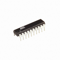
ATTINY2313A-PU Atmel, ATTINY2313A-PU Datasheet - Page 10

ATTINY2313A-PU
Manufacturer Part Number
ATTINY2313A-PU
Description
IC MCU AVR 2K FLASH 20MHZ 20DIP
Manufacturer
Atmel
Series
AVR® ATtinyr
Specifications of ATTINY2313A-PU
Core Processor
AVR
Core Size
8-Bit
Speed
20MHz
Connectivity
I²C, SPI, UART/USART
Peripherals
Brown-out Detect/Reset, POR, PWM, WDT
Number Of I /o
18
Program Memory Size
2KB (1K x 16)
Program Memory Type
FLASH
Eeprom Size
128 x 8
Ram Size
128 x 8
Voltage - Supply (vcc/vdd)
1.8 V ~ 5.5 V
Oscillator Type
Internal
Operating Temperature
-40°C ~ 85°C
Package / Case
20-DIP (0.300", 7.62mm)
Processor Series
ATTINY2x
Core
AVR8
Data Bus Width
8 bit
Data Ram Size
128 B
Interface Type
SPI, USART
Maximum Clock Frequency
20 MHz
Number Of Programmable I/os
18
Operating Supply Voltage
1.8 V to 5.5 V
Maximum Operating Temperature
+ 85 C
Mounting Style
Through Hole
3rd Party Development Tools
EWAVR, EWAVR-BL
Development Tools By Supplier
ATAVRDRAGON, ATSTK500, ATSTK600, ATAVRISP2, ATAVRONEKIT
Minimum Operating Temperature
- 40 C
Controller Family/series
ATtiny
No. Of I/o's
18
Eeprom Memory Size
128Byte
Ram Memory Size
128Byte
Cpu Speed
20MHz
Rohs Compliant
Yes
Lead Free Status / RoHS Status
Lead free / RoHS Compliant
Data Converters
-
Lead Free Status / Rohs Status
Lead free / RoHS Compliant
Available stocks
Company
Part Number
Manufacturer
Quantity
Price
Company:
Part Number:
ATTINY2313A-PU
Manufacturer:
TI
Quantity:
1 560
Part Number:
ATTINY2313A-PU
Manufacturer:
ATMEL/爱特梅尔
Quantity:
20 000
10
ROR
ASR
SWAP
BSET
BCLR
BST
BLD
SEC
CLC
SEN
CLN
SEZ
CLZ
SEI
CLI
SES
CLS
SEV
CLV
SET
CLT
SEH
CLH
DATA TRANSFER INSTRUCTIONS
MOV
MOVW
LDI
LD
LD
LD
LD
LD
LD
LDD
LD
LD
LD
LDD
LDS
ST
ST
ST
ST
ST
ST
STD
ST
ST
ST
STD
STS
LPM
LPM
LPM
SPM
IN
OUT
PUSH
POP
MCU CONTROL INSTRUCTIONS
NOP
SLEEP
WDR
BREAK
Mnemonics
ATtiny2313A/4313
Rd
Rd
Rd
s
s
Rr, b
Rd, b
Rd, Rr
Rd, Rr
Rd, K
Rd, X
Rd, X+
Rd, - X
Rd, Y
Rd, Y+
Rd, - Y
Rd,Y+q
Rd, Z
Rd, Z+
Rd, -Z
Rd, Z+q
Rd, k
X, Rr
X+, Rr
- X, Rr
Y, Rr
Y+, Rr
- Y, Rr
Y+q,Rr
Z, Rr
Z+, Rr
-Z, Rr
Z+q,Rr
k, Rr
Rd, Z
Rd, Z+
Rd, P
P, Rr
Rr
Rd
Operands
Rotate Right Through Carry
Arithmetic Shift Right
Swap Nibbles
Flag Set
Flag Clear
Bit Store from Register to T
Bit load from T to Register
Set Carry
Clear Carry
Set Negative Flag
Clear Negative Flag
Set Zero Flag
Clear Zero Flag
Global Interrupt Enable
Global Interrupt Disable
Set Signed Test Flag
Clear Signed Test Flag
Set Twos Complement Overflow.
Clear Twos Complement Overflow
Set T in SREG
Clear T in SREG
Set Half Carry Flag in SREG
Clear Half Carry Flag in SREG
Move Between Registers
Copy Register Word
Load Immediate
Load Indirect
Load Indirect and Post-Inc.
Load Indirect and Pre-Dec.
Load Indirect
Load Indirect and Post-Inc.
Load Indirect and Pre-Dec.
Load Indirect with Displacement
Load Indirect
Load Indirect and Post-Inc.
Load Indirect and Pre-Dec.
Load Indirect with Displacement
Load Direct from SRAM
Store Indirect
Store Indirect and Post-Inc.
Store Indirect and Pre-Dec.
Store Indirect
Store Indirect and Post-Inc.
Store Indirect and Pre-Dec.
Store Indirect with Displacement
Store Indirect
Store Indirect and Post-Inc.
Store Indirect and Pre-Dec.
Store Indirect with Displacement
Store Direct to SRAM
Load Program Memory
Load Program Memory
Load Program Memory and Post-Inc
Store Program Memory
In Port
Out Port
Push Register on Stack
Pop Register from Stack
No Operation
Sleep
Watchdog Reset
Break
Description
Rd(7)←C,Rd(n)← Rd(n+1),C←Rd(0)
Rd(n) ← Rd(n+1), n=0..6
Rd(3..0)←Rd(7..4),Rd(7..4)←Rd(3..0)
SREG(s) ← 1
SREG(s) ← 0
T ← Rr(b)
Rd(b) ← T
C ← 1
C ← 0
N ← 1
N ← 0
Z ← 1
Z ← 0
I ← 1
I ← 0
S ← 1
S ← 0
V ← 1
V ← 0
T ← 1
T ← 0
H ← 1
H ← 0
Rd ← Rr
Rd+1:Rd ← Rr+1:Rr
Rd ← K
Rd ← (X)
Rd ← (X), X ← X + 1
X ← X - 1, Rd ← (X)
Rd ← (Y)
Rd ← (Y), Y ← Y + 1
Y ← Y - 1, Rd ← (Y)
Rd ← (Y + q)
Rd ← (Z)
Rd ← (Z), Z ← Z+1
Z ← Z - 1, Rd ← (Z)
Rd ← (Z + q)
Rd ← (k)
(X) ← Rr
(X) ← Rr, X ← X + 1
X ← X - 1, (X) ← Rr
(Y) ← Rr
(Y) ← Rr, Y ← Y + 1
Y ← Y - 1, (Y) ← Rr
(Y + q) ← Rr
(Z) ← Rr
(Z) ← Rr, Z ← Z + 1
Z ← Z - 1, (Z) ← Rr
(Z + q) ← Rr
(k) ← Rr
R0 ← (Z)
Rd ← (Z)
Rd ← (Z), Z ← Z+1
(Z) ← R1:R0
Rd ← P
P ← Rr
STACK ← Rr
Rd ← STACK
(see specific descr. for Sleep function)
(see specific descr. for WDR/timer)
For On-chip Debug Only
Operation
Z,C,N,V
Z,C,N,V
None
SREG(s)
SREG(s)
T
None
C
C
N
N
Z
Z
I
I
S
S
V
V
T
T
H
H
None
None
None
None
None
None
None
None
None
None
None
None
None
None
None
None
None
None
None
None
None
None
None
None
None
None
None
None
None
None
None
None
None
None
None
None
None
None
None
Flags
8246AS–AVR–11/09
#Clocks
N/A
1
1
1
1
1
1
1
1
1
1
1
1
1
1
1
1
1
1
1
1
1
1
1
1
1
1
2
2
2
2
2
2
2
2
2
2
2
2
2
2
2
2
2
2
2
2
2
2
2
2
3
3
3
1
1
2
2
1
1
1
-


