ATMEGA48-20MU Atmel, ATMEGA48-20MU Datasheet - Page 18
ATMEGA48-20MU
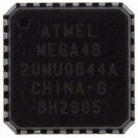
Manufacturer Part Number
ATMEGA48-20MU
Description
IC AVR MCU 4K 20MHZ 5V 32-QFN
Manufacturer
Atmel
Series
AVR® ATmegar
Specifications of ATMEGA48-20MU
Core Processor
AVR
Core Size
8-Bit
Speed
20MHz
Connectivity
I²C, SPI, UART/USART
Peripherals
Brown-out Detect/Reset, POR, PWM, WDT
Number Of I /o
23
Program Memory Size
4KB (2K x 16)
Program Memory Type
FLASH
Eeprom Size
256 x 8
Ram Size
512 x 8
Voltage - Supply (vcc/vdd)
2.7 V ~ 5.5 V
Data Converters
A/D 8x10b
Oscillator Type
Internal
Operating Temperature
-40°C ~ 85°C
Package / Case
32-VQFN Exposed Pad, 32-HVQFN, 32-SQFN, 32-DHVQFN
Processor Series
ATMEGA48x
Core
AVR8
Data Bus Width
8 bit
Data Ram Size
512 B
Interface Type
2-Wire/SPI/USART/Serial
Maximum Clock Frequency
20 MHz
Number Of Programmable I/os
23
Number Of Timers
3
Operating Supply Voltage
2.7 V to 5.5 V
Maximum Operating Temperature
+ 85 C
Mounting Style
SMD/SMT
3rd Party Development Tools
EWAVR, EWAVR-BL
Development Tools By Supplier
ATAVRDRAGON, ATSTK500, ATSTK600, ATAVRISP2, ATAVRONEKIT
Minimum Operating Temperature
- 40 C
On-chip Adc
8-ch x 10-bit
Controller Family/series
AVR MEGA
No. Of I/o's
23
Eeprom Memory Size
256Byte
Ram Memory Size
512Byte
Cpu Speed
20MHz
No. Of Timers
3
Rohs Compliant
Yes
Package
32MLF EP
Device Core
AVR
Family Name
ATmega
Maximum Speed
20 MHz
For Use With
ATSTK600-TQFP32 - STK600 SOCKET/ADAPTER 32-TQFPATSTK600-DIP40 - STK600 SOCKET/ADAPTER 40-PDIP770-1007 - ISP 4PORT ATMEL AVR MCU SPI/JTAGATAVRDRAGON - KIT DRAGON 32KB FLASH MEM AVRATAVRISP2 - PROGRAMMER AVR IN SYSTEMATJTAGICE2 - AVR ON-CHIP D-BUG SYSTEM
Lead Free Status / RoHS Status
Lead free / RoHS Compliant
Available stocks
Company
Part Number
Manufacturer
Quantity
Price
Company:

Part Number:
ATMEGA48-20MU
Manufacturer:
ATMEL
Quantity:
18 000


7.3
7.3.1
18
SRAM Data Memory
ATmega48/88/168
Data Memory Access Times
Figure 7-3
The ATmega48/88/168 is a complex microcontroller with more peripheral units than can be sup-
ported within the 64 locations reserved in the Opcode for the IN and OUT instructions. For the
Extended I/O space from 0x60 - 0xFF in SRAM, only the ST/STS/STD and LD/LDS/LDD instruc-
tions can be used.
The lower 768/1280/1280 data memory locations address both the Register File, the I/O mem-
ory, Extended I/O memory, and the internal data SRAM. The first 32 locations address the
Register File, the next 64 location the standard I/O memory, then 160 locations of Extended I/O
memory, and the next 512/1024/1024 locations address the internal data SRAM.
The five different addressing modes for the data memory cover: Direct, Indirect with Displace-
ment, Indirect, Indirect with Pre-decrement, and Indirect with Post-increment. In the Register
File, registers R26 to R31 feature the indirect addressing pointer registers.
The direct addressing reaches the entire data space.
The Indirect with Displacement mode reaches 63 address locations from the base address given
by the Y-register or Z-register.
When using register indirect addressing modes with automatic pre-decrement and post-incre-
ment, the address registers X, Y, and Z are decremented or incremented.
The 32 general purpose working registers, 64 I/O Registers, 160 Extended I/O Registers, and
the 512/1024/1024 bytes of internal data SRAM in the ATmega48/88/168 are all accessible
through all these addressing modes. The Register File is described in
ter File” on page
Figure 7-3.
This section describes the general access timing concepts for internal memory access. The
internal data SRAM access is performed in two clk
shows how the ATmega48/88/168 SRAM Memory is organized.
Data Memory Map
11.
(512/1024/1024 x 8)
160 Ext I/O Reg.
64 I/O Registers
Data Memory
Internal SRAM
32 Registers
0x02FF/0x04FF/0x04FF
0x0000 - 0x001F
0x0020 - 0x005F
0x0060 - 0x00FF
0x0100
CPU
cycles as described in
“General Purpose Regis-
Figure
2545S–AVR–07/10
7-4.
Related parts for ATMEGA48-20MU
Image
Part Number
Description
Manufacturer
Datasheet
Request
R

Part Number:
Description:
IC AVR MCU 4K 5V 20MHZ 32-TQFP
Manufacturer:
Atmel
Datasheet:

Part Number:
Description:
Manufacturer:
Atmel Corporation
Datasheet:
Part Number:
Description:
Manufacturer:
Atmel Corporation
Datasheet:
Part Number:
Description:
IC AVR MCU 4K 20MHZ 5V 32TQFP
Manufacturer:
Atmel
Datasheet:

Part Number:
Description:
IC AVR MCU 4K 20MHZ 5V 28DIP
Manufacturer:
Atmel
Datasheet:

Part Number:
Description:
IC AVR MCU 4K 5V 20MHZ 32-TQFP
Manufacturer:
Atmel
Datasheet:

Part Number:
Description:
IC AVR MCU 4K 5V 20MHZ 32-QFN
Manufacturer:
Atmel
Datasheet:
Part Number:
Description:
IC AVR MCU 4K 5V 20MHZ 32-QFN
Manufacturer:
Atmel
Datasheet:
Part Number:
Description:
IC AVR MCU 4K 5V 20MHZ 28-DIP
Manufacturer:
Atmel
Datasheet:
Part Number:
Description:
IC AVR MCU 4K 5V 20MHZ 28-DIP
Manufacturer:
Atmel
Datasheet:

Part Number:
Description:
IC AVR MCU 4K FLASH 20MHZ 28QFN
Manufacturer:
Atmel
Datasheet:
Part Number:
Description:
MCU AVR 4KB FLASH 20MHZ 32QFN
Manufacturer:
Atmel
Datasheet: