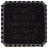
ATMEGA48-20MU Atmel, ATMEGA48-20MU Datasheet - Page 209

ATMEGA48-20MU
Manufacturer Part Number
ATMEGA48-20MU
Description
IC AVR MCU 4K 20MHZ 5V 32-QFN
Manufacturer
Atmel
Series
AVR® ATmegar
Specifications of ATMEGA48-20MU
Core Processor
AVR
Core Size
8-Bit
Speed
20MHz
Connectivity
I²C, SPI, UART/USART
Peripherals
Brown-out Detect/Reset, POR, PWM, WDT
Number Of I /o
23
Program Memory Size
4KB (2K x 16)
Program Memory Type
FLASH
Eeprom Size
256 x 8
Ram Size
512 x 8
Voltage - Supply (vcc/vdd)
2.7 V ~ 5.5 V
Data Converters
A/D 8x10b
Oscillator Type
Internal
Operating Temperature
-40°C ~ 85°C
Package / Case
32-VQFN Exposed Pad, 32-HVQFN, 32-SQFN, 32-DHVQFN
Processor Series
ATMEGA48x
Core
AVR8
Data Bus Width
8 bit
Data Ram Size
512 B
Interface Type
2-Wire/SPI/USART/Serial
Maximum Clock Frequency
20 MHz
Number Of Programmable I/os
23
Number Of Timers
3
Operating Supply Voltage
2.7 V to 5.5 V
Maximum Operating Temperature
+ 85 C
Mounting Style
SMD/SMT
3rd Party Development Tools
EWAVR, EWAVR-BL
Development Tools By Supplier
ATAVRDRAGON, ATSTK500, ATSTK600, ATAVRISP2, ATAVRONEKIT
Minimum Operating Temperature
- 40 C
On-chip Adc
8-ch x 10-bit
Controller Family/series
AVR MEGA
No. Of I/o's
23
Eeprom Memory Size
256Byte
Ram Memory Size
512Byte
Cpu Speed
20MHz
No. Of Timers
3
Rohs Compliant
Yes
Package
32MLF EP
Device Core
AVR
Family Name
ATmega
Maximum Speed
20 MHz
For Use With
ATSTK600-TQFP32 - STK600 SOCKET/ADAPTER 32-TQFPATSTK600-DIP40 - STK600 SOCKET/ADAPTER 40-PDIP770-1007 - ISP 4PORT ATMEL AVR MCU SPI/JTAGATAVRDRAGON - KIT DRAGON 32KB FLASH MEM AVRATAVRISP2 - PROGRAMMER AVR IN SYSTEMATJTAGICE2 - AVR ON-CHIP D-BUG SYSTEM
Lead Free Status / RoHS Status
Lead free / RoHS Compliant
Available stocks
Company
Part Number
Manufacturer
Quantity
Price
Company:
Part Number:
ATMEGA48-20MU
Manufacturer:
ATMEL
Quantity:
18 000
- Current page: 209 of 378
- Download datasheet (8Mb)
21.2.2
21.3
21.3.1
21.3.2
2545S–AVR–07/10
Data Transfer and Frame Format
Electrical Interconnection
Transferring Bits
START and STOP Conditions
Table 21-1.
The PRTWI bit in
the 2-wire Serial Interface.
As depicted in
pull-up resistors. The bus drivers of all TWI-compliant devices are open-drain or open-collector.
This implements a wired-AND function which is essential to the operation of the interface. A low
level on a TWI bus line is generated when one or more TWI devices output a zero. A high level
is output when all TWI devices tri-state their outputs, allowing the pull-up resistors to pull the line
high. Note that all AVR devices connected to the TWI bus must be powered in order to allow any
bus operation.
The number of devices that can be connected to the bus is only limited by the bus capacitance
limit of 400 pF and the 7-bit slave address space. A detailed specification of the electrical char-
acteristics of the TWI is given in
different sets of specifications are presented there, one relevant for bus speeds below 100 kHz,
and one valid for bus speeds up to 400 kHz.
Each data bit transferred on the TWI bus is accompanied by a pulse on the clock line. The level
of the data line must be stable when the clock line is high. The only exception to this rule is for
generating start and stop conditions.
Figure 21-2. Data Validity
The Master initiates and terminates a data transmission. The transmission is initiated when the
Master issues a START condition on the bus, and it is terminated when the Master issues a
STOP condition. Between a START and a STOP condition, the bus is considered busy, and no
Term
Slave
Transmitter
Receiver
SDA
SCL
TWI Terminology
Figure
Description
The device addressed by a Master.
The device placing data on the bus.
The device reading data from the bus.
“Minimizing Power Consumption” on page 40
21-1, both bus lines are connected to the positive supply voltage through
Data Stable
“2-wire Serial Interface Characteristics” on page
Data Change
Data Stable
ATmega48/88/168
must be written to zero to enable
307. Two
209
Related parts for ATMEGA48-20MU
Image
Part Number
Description
Manufacturer
Datasheet
Request
R

Part Number:
Description:
IC AVR MCU 4K 5V 20MHZ 32-TQFP
Manufacturer:
Atmel
Datasheet:

Part Number:
Description:
Manufacturer:
Atmel Corporation
Datasheet:

Part Number:
Description:
Manufacturer:
Atmel Corporation
Datasheet:

Part Number:
Description:
IC AVR MCU 4K 20MHZ 5V 32TQFP
Manufacturer:
Atmel
Datasheet:

Part Number:
Description:
IC AVR MCU 4K 20MHZ 5V 28DIP
Manufacturer:
Atmel
Datasheet:

Part Number:
Description:
IC AVR MCU 4K 5V 20MHZ 32-TQFP
Manufacturer:
Atmel
Datasheet:

Part Number:
Description:
IC AVR MCU 4K 5V 20MHZ 32-QFN
Manufacturer:
Atmel
Datasheet:

Part Number:
Description:
IC AVR MCU 4K 5V 20MHZ 32-QFN
Manufacturer:
Atmel
Datasheet:

Part Number:
Description:
IC AVR MCU 4K 5V 20MHZ 28-DIP
Manufacturer:
Atmel
Datasheet:

Part Number:
Description:
IC AVR MCU 4K 5V 20MHZ 28-DIP
Manufacturer:
Atmel
Datasheet:

Part Number:
Description:
IC AVR MCU 4K FLASH 20MHZ 28QFN
Manufacturer:
Atmel
Datasheet:

Part Number:
Description:
MCU AVR 4KB FLASH 20MHZ 32QFN
Manufacturer:
Atmel
Datasheet:


