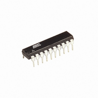
ATTINY26-16PU Atmel, ATTINY26-16PU Datasheet - Page 5

ATTINY26-16PU
Manufacturer Part Number
ATTINY26-16PU
Description
IC AVR MCU 2K 16MHZ IND 20-DIP
Manufacturer
Atmel
Series
AVR® ATtinyr
Specifications of ATTINY26-16PU
Core Processor
AVR
Core Size
8-Bit
Speed
16MHz
Connectivity
USI
Peripherals
Brown-out Detect/Reset, POR, PWM, WDT
Number Of I /o
16
Program Memory Size
2KB (1K x 16)
Program Memory Type
FLASH
Eeprom Size
128 x 8
Ram Size
128 x 8
Voltage - Supply (vcc/vdd)
4.5 V ~ 5.5 V
Data Converters
A/D 11x10b
Oscillator Type
Internal
Operating Temperature
-40°C ~ 85°C
Package / Case
20-DIP (0.300", 7.62mm)
Processor Series
ATTINY2x
Core
AVR8
Data Bus Width
8 bit
Data Ram Size
128 B
Interface Type
2-Wire/ISP/SM-Bus/SPI/UART/USI
Maximum Clock Frequency
16 MHz
Number Of Programmable I/os
16
Number Of Timers
2
Operating Supply Voltage
4.5 V to 5.5 V
Maximum Operating Temperature
+ 85 C
Mounting Style
Through Hole
3rd Party Development Tools
EWAVR, EWAVR-BL
Development Tools By Supplier
ATAVRDRAGON, ATSTK500, ATSTK600, ATAVRISP2, ATAVRONEKIT
Minimum Operating Temperature
- 40 C
On-chip Adc
11-ch x 10-bit
Package
20PDIP
Device Core
AVR
Family Name
ATtiny
Maximum Speed
16 MHz
For Use With
ATSTK600 - DEV KIT FOR AVR/AVR32770-1007 - ISP 4PORT ATMEL AVR MCU SPI/JTAGATAVRISP2 - PROGRAMMER AVR IN SYSTEMATSTK505 - ADAPTER KIT FOR 14PIN AVR MCU
Lead Free Status / RoHS Status
Lead free / RoHS Compliant
Pin Descriptions
VCC
GND
AVCC
Port A (PA7..PA0)
Port B (PB7..PB0)
XTAL1
XTAL2
1477KS–AVR–08/10
Digital supply voltage pin.
Digital ground pin.
AVCC is the supply voltage pin for Port A and the A/D Converter (ADC). It should be externally
connected to V
through a low-pass filter. See page 94 for details on operating of the ADC.
Port A is an 8-bit general purpose I/O port. PA7..PA0 are all I/O pins that can provide internal
pull-ups (selected for each bit). Port A has alternate functions as analog inputs for the ADC and
analog comparator and pin change interrupt as described in “Alternate Port Functions” on page
46.
Port B is an 8-bit general purpose I/O port. PB6..0 are all I/O pins that can provide internal pull-
ups (selected for each bit). PB7 is an I/O pin if not used as the reset. To use pin PB7 as an I/O
pin, instead of RESET pin, program (“0”) RSTDISBL Fuse. Port B has alternate functions for the
ADC, clocking, timer counters, USI, SPI programming, and pin change interrupt as described in
“Alternate Port Functions” on page 46.
An External Reset is generated by a low level on the PB7/RESET pin. Reset pulses longer than
50 ns will generate a reset, even if the clock is not running. Shorter pulses are not guaranteed to
generate a reset.
Input to the inverting oscillator amplifier and input to the internal clock operating circuit.
Output from the inverting oscillator amplifier.
CC
, even if the ADC is not used. If the ADC is used, it should be connected to V
CC
5


