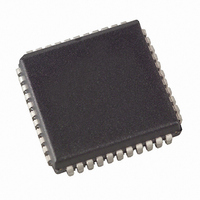
AT89C51RC-24JU Atmel, AT89C51RC-24JU Datasheet - Page 4

AT89C51RC-24JU
Manufacturer Part Number
AT89C51RC-24JU
Description
IC 8051 MCU FLASH 32K 44PLCC
Manufacturer
Atmel
Series
89Cr
Datasheet
1.AT89C51RC-24PU.pdf
(36 pages)
Specifications of AT89C51RC-24JU
Core Processor
8051
Core Size
8-Bit
Speed
24MHz
Connectivity
SPI, UART/USART
Peripherals
WDT
Number Of I /o
32
Program Memory Size
32KB (32K x 8)
Program Memory Type
FLASH
Ram Size
512 x 8
Voltage - Supply (vcc/vdd)
4 V ~ 5.5 V
Oscillator Type
Internal
Operating Temperature
-40°C ~ 85°C
Package / Case
44-PLCC
Package
44PLCC
Device Core
8051
Family Name
89C
Maximum Speed
24 MHz
Operating Supply Voltage
5 V
Data Bus Width
8 Bit
Number Of Programmable I/os
32
Interface Type
UART
Number Of Timers
3
Processor Series
AT89x
Core
8051
Data Ram Size
512 B
Maximum Clock Frequency
33 MHz
Maximum Operating Temperature
+ 85 C
Mounting Style
SMD/SMT
3rd Party Development Tools
PK51, CA51, A51, ULINK2
Minimum Operating Temperature
- 40 C
For Use With
AT89STK-11 - KIT STARTER FOR AT89C51RX2
Lead Free Status / RoHS Status
Lead free / RoHS Compliant
Eeprom Size
-
Data Converters
-
Lead Free Status / Rohs Status
Details
Available stocks
Company
Part Number
Manufacturer
Quantity
Price
Company:
Part Number:
AT89C51RC-24JU
Manufacturer:
ATMEL
Quantity:
34 960
Company:
Part Number:
AT89C51RC-24JU
Manufacturer:
ATMEL
Quantity:
5 000
Part Number:
AT89C51RC-24JU
Manufacturer:
ATMEL/爱特梅尔
Quantity:
20 000
4. Pin Description
4.1
4.2
4.3
4.4
4.5
4
VCC
GND
Port 0
Port 1
Port 2
AT89C51RC
Supply voltage.
Ground.
Port 0 is an 8-bit open drain bi-directional I/O port. As an output port, each pin can sink eight TTL
inputs. When 1s are written to port 0 pins, the pins can be used as high-impedance inputs.
Port 0 can also be configured to be the multiplexed low-order address/data bus during accesses
to external program and data memory. In this mode, P0 has internal pull-ups.
Port 0 also receives the code bytes during Flash programming and outputs the code bytes dur-
ing program verification. External pull-ups are required during program verification.
Port 1 is an 8-bit bi-directional I/O port with internal pull-ups. The Port 1 output buffers can
sink/source four TTL inputs. When 1s are written to Port 1 pins, they are pulled high by the inter-
nal pull-ups and can be used as inputs. As inputs, Port 1 pins that are externally being pulled low
will source current (I
In addition, P1.0 and P1.1 can be configured to be the timer/counter 2 external count input
(P1.0/T2) and the timer/counter 2 trigger input (P1.1/T2EX), respectively, as shown in the follow-
ing table.
Port 1 also receives the low-order address bytes during Flash programming and verification.
Port 2 is an 8-bit bi-directional I/O port with internal pull-ups. The Port 2 output buffers can
sink/source four TTL inputs. When 1s are written to Port 2 pins, they are pulled high by the inter-
nal pull-ups and can be used as inputs. As inputs, Port 2 pins that are externally being pulled low
will source current (I
Port 2 emits the high-order address byte during fetches from external program memory and dur-
ing accesses to external data memory that use 16-bit addresses (MOVX @ DPTR). In this
application, Port 2 uses strong internal pull-ups when emitting 1s. During accesses to external
data memory that use 8-bit addresses (MOVX @ RI), Port 2 emits the contents of the P2 Special
Function Register.
Port 2 also receives the high-order address bits and some control signals during Flash program-
ming and verification.
Port Pin
P1.0
P1.1
IL
IL
) because of the internal pull-ups.
) because of the internal pull-ups.
Alternate Functions
T2 (external count input to Timer/Counter 2), clock-out
T2EX (Timer/Counter 2 capture/reload trigger and direction control)
1920D–MICRO–6/08


