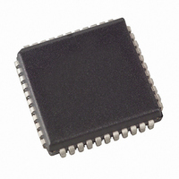
AT89C51RD2-SLSUM Atmel, AT89C51RD2-SLSUM Datasheet - Page 13

AT89C51RD2-SLSUM
Manufacturer Part Number
AT89C51RD2-SLSUM
Description
IC 8051 MCU FLASH 64K 44PLCC
Manufacturer
Atmel
Series
89Cr
Datasheet
1.ATWEBDVK-02RC.pdf
(137 pages)
Specifications of AT89C51RD2-SLSUM
Core Processor
8051
Core Size
8-Bit
Speed
60MHz
Connectivity
SPI, UART/USART
Peripherals
POR, PWM, WDT
Number Of I /o
34
Program Memory Size
64KB (64K x 8)
Program Memory Type
FLASH
Ram Size
2K x 8
Voltage - Supply (vcc/vdd)
2.7 V ~ 5.5 V
Oscillator Type
External
Operating Temperature
-40°C ~ 85°C
Package / Case
44-PLCC
Processor Series
AT89x
Core
8051
Data Bus Width
8 bit
Data Ram Size
2 KB
Interface Type
UART, SPI
Maximum Clock Frequency
60 MHz
Number Of Programmable I/os
32
Number Of Timers
3
Operating Supply Voltage
2.7 V to 5.5 V
Maximum Operating Temperature
+ 85 C
Mounting Style
SMD/SMT
3rd Party Development Tools
PK51, CA51, A51, ULINK2
Minimum Operating Temperature
- 40 C
Package
44PLCC
Device Core
80C51
Family Name
89C
Maximum Speed
40 MHz
For Use With
AT89OCD-01 - USB EMULATOR FOR AT8XC51 MCUAT89STK-11 - KIT STARTER FOR AT89C51RX2
Lead Free Status / RoHS Status
Lead free / RoHS Compliant
Eeprom Size
-
Data Converters
-
Lead Free Status / Rohs Status
Details
Available stocks
Company
Part Number
Manufacturer
Quantity
Price
Company:
Part Number:
AT89C51RD2-SLSUM
Manufacturer:
ATMEL
Quantity:
185 248
Company:
Part Number:
AT89C51RD2-SLSUM
Manufacturer:
CMD
Quantity:
1 993
Part Number:
AT89C51RD2-SLSUM
Manufacturer:
MICROCHIP/微芯
Quantity:
20 000
Table 4-1.
4235K–8051–05/08
ALE/PRO
G
PSEN
EA
Mnemonic
Pin Description (Continued)
PLCC44 VQFP44
33
32
35
27
26
29
Pin Number
PLCC68
68
67
2
VQFP64
56
55
58
Type
O (I)
O
I
Name and Function
Address Latch Enable/Program Pulse: Output pulse for latching the
low byte of the address during an access to external memory. In normal
operation, ALE is emitted at a constant rate of 1/6 (1/3 in X2 mode) the
oscillator frequency, and can be used for external timing or clocking. Note
that one ALE pulse is skipped during each access to external data
memory. This pin is also the program pulse input (PROG) during Flash
programming. ALE can be disabled by setting SFR’s AUXR.0 bit. With
this bit set, ALE will be inactive during internal fetches.
Program Strobe ENable: The read strobe to external program memory.
When executing code from the external program memory, PSEN is
activated twice each machine cycle, except that two PSEN activations
are skipped during each access to external data memory. PSEN is not
activated during fetches from internal program memory.
External Access Enable: EA must be externally held low to enable the
device to fetch code from external program memory locations 0000H to
FFFFH. If security level 1 is programmed, EA will be internally latched on
Reset.
AT89C51RD2/ED2
13


