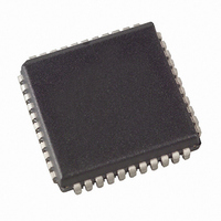
AT89C51RD2-SLSUM Atmel, AT89C51RD2-SLSUM Datasheet - Page 35

AT89C51RD2-SLSUM
Manufacturer Part Number
AT89C51RD2-SLSUM
Description
IC 8051 MCU FLASH 64K 44PLCC
Manufacturer
Atmel
Series
89Cr
Datasheet
1.ATWEBDVK-02RC.pdf
(137 pages)
Specifications of AT89C51RD2-SLSUM
Core Processor
8051
Core Size
8-Bit
Speed
60MHz
Connectivity
SPI, UART/USART
Peripherals
POR, PWM, WDT
Number Of I /o
34
Program Memory Size
64KB (64K x 8)
Program Memory Type
FLASH
Ram Size
2K x 8
Voltage - Supply (vcc/vdd)
2.7 V ~ 5.5 V
Oscillator Type
External
Operating Temperature
-40°C ~ 85°C
Package / Case
44-PLCC
Processor Series
AT89x
Core
8051
Data Bus Width
8 bit
Data Ram Size
2 KB
Interface Type
UART, SPI
Maximum Clock Frequency
60 MHz
Number Of Programmable I/os
32
Number Of Timers
3
Operating Supply Voltage
2.7 V to 5.5 V
Maximum Operating Temperature
+ 85 C
Mounting Style
SMD/SMT
3rd Party Development Tools
PK51, CA51, A51, ULINK2
Minimum Operating Temperature
- 40 C
Package
44PLCC
Device Core
80C51
Family Name
89C
Maximum Speed
40 MHz
For Use With
AT89OCD-01 - USB EMULATOR FOR AT8XC51 MCUAT89STK-11 - KIT STARTER FOR AT89C51RX2
Lead Free Status / RoHS Status
Lead free / RoHS Compliant
Eeprom Size
-
Data Converters
-
Lead Free Status / Rohs Status
Details
Available stocks
Company
Part Number
Manufacturer
Quantity
Price
Company:
Part Number:
AT89C51RD2-SLSUM
Manufacturer:
ATMEL
Quantity:
185 248
Company:
Part Number:
AT89C51RD2-SLSUM
Manufacturer:
CMD
Quantity:
1 993
Part Number:
AT89C51RD2-SLSUM
Manufacturer:
MICROCHIP/微芯
Quantity:
20 000
13. Programmable Counter Array (PCA)
4235K–8051–05/08
The PCA provides more timing capabilities with less CPU intervention than the standard
timer/counters. Its advantages include reduced software overhead and improved accuracy. The
PCA consists of a dedicated timer/counter which serves as the time base for an array of five
compare/capture modules. Its clock input can be programmed to count any one of the following
signals:
Each compare/capture module can be programmed in any one of the following modes:
Module 4 can also be programmed as a watchdog timer (see Section "PCA Watchdog Timer",
page 46).
When the compare/capture modules are programmed in the capture mode, software timer, or
high speed output mode, an interrupt can be generated when the module executes its function.
All five modules plus the PCA timer overflow share one interrupt vector.
The PCA timer/counter and compare/capture modules share Port 1 for external I/O. These pins
are listed below. If one or several bits in the port are not used for the PCA, they can still be used
for standard I/O.
The PCA timer is a common time base for all five modules (see Figure 13-1). The timer count
source is determined from the CPS1 and CPS0 bits in the CMOD register (Table 13-1) and can
be programmed to run at:
The CMOD register includes three additional bits associated with the PCA (See Figure 13-1 and
Table 13-1).
• Peripheral clock frequency (F
• Peripheral clock frequency (F
• Timer 0 overflow
• External input on ECI (P1.2)
• Rising and/or falling edge capture
• Software timer
• High-speed output
• Pulse width modulator
• 1/6 the
• 1/2 the
• The Timer 0 overflow
• The input on the ECI pin (P1.2)
• The CIDL bit which allows the PCA to stop during idle mode.
• The WDTE bit which enables or disables the watchdog function on module 4.
peripheral clock frequency (F
peripheral clock frequency (F
PCA Component
16-bit Module 0
16-bit Module 1
16-bit Module 2
16-bit Module 3
16-bit Counter
CLK PERIPH
CLK PERIPH
)
)
CLK PERIPH
CLK PERIPH
÷
÷
2
6
)
)
AT89C51RD2/ED2
External I/O Pin
P1.3/CEX0
P1.4/CEX1
P1.5/CEX2
P1.6/CEX3
P1.2/ECI
35


